
Semiconductor Electronics
Get insights from 56 questions on Semiconductor Electronics, answered by students, alumni, and experts. You may also ask and answer any question you like about Semiconductor Electronics
- 56
Questions
- 0
Discussions
- 0
Active Users
- 0
Followers
Have a question about Semiconductor Electronics? Ask our experts
Keep it short & simple. Type complete word. Avoid abusive language.
The output of the given circuit in figure is given below.
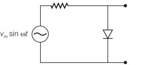
(c) Would be like a half wave rectifier with negative cycles in output
(d) Would be like that of a full wave rectifier
The output of the given circuit in figure is given below.

(c) Would be like a half wave rectifier with negative cycles in output
(d) Would be like that of a full wave rectifier
This is a Multiple Choice Questions as classified in NCERT Exemplar
Answer- c
Explanation- due to forward biasing the diffusion current in the circuit is very high and resistance in the circuit is very low. Thus voltage across pn junction is very low but in case of reverse biasing diffusion current ve
 Upvote

Hole is
(a) An anti-particle of electron
(b) A vacancy created when an electron leaves a covalent bond
(c) Absence of free electrons
(d) An artificially created particle
Hole is
(a) An anti-particle of electron
(b) A vacancy created when an electron leaves a covalent bond
(c) Absence of free electrons
(d) An artificially created particle
This is a Multiple Choice Questions as classified in NCERT Exemplar
Answer-b
Explanation -when a neutral entity is there it contains both equal number of elctron and holes. Also when electron emit from neutral entity then it leave behind a vacancy that is hole.
Upvote <p><strong> Hole is </strong><br><strong>(a)</strong> An anti-particle of electron<br><strong>(b)</strong> A vacancy created when an electron leaves a covalent bond<br><strong>(c) </strong>Absence of free electrons<br><strong>(d)</strong> An artificially created particle</p>
A 220 V AC supply is connected between points A and B (figure). What will be the potential difference V across the capacitor?
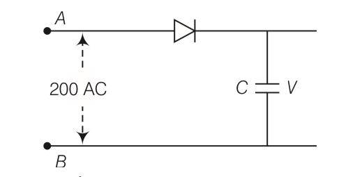
A 220 V AC supply is connected between points A and B (figure). What will be the potential difference V across the capacitor?

This is a Multiple Choice Questions as classified in NCERT Exemplar
Answer- d
Explanation- as we know that Ev = Eo/ so E0= Ev so net voltage is 220 V
Upvote In figure given on next page, assuming the diodes to be ideal
(a) D1is forward biased and D2 is reverse biased and hence current flows from A to B
(b) D2 is forward biased and D1 is reverse biased and hence no current flows from B to A and vice-versa
(c) D1 and D2 are both forward biased and hence current flows from A to B
(d) D1 and D2 are both reverse biased and hence no current flows from A to B and vice-versa
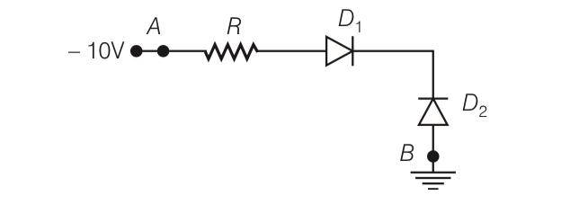
In figure given on next page, assuming the diodes to be ideal
(a) D1is forward biased and D2 is reverse biased and hence current flows from A to B
(b) D2 is forward biased and D1 is reverse biased and hence no current flows from B to A and vice-versa
(c) D1 and D2 are both forward biased and hence current flows from A to B
(d) D1 and D2 are both reverse biased and hence no current flows from A to B and vice-versa

This is a Multiple Choice Questions as classified in NCERT Exemplar
Answer-b
Explanation- from the figure we can say that diode D1 is reverse biased and diode D2 is forward biased so current will flow from B to A.
Upvote In figure given below V0 is the potential barrier across a pn junction when no battery is connected across the junction
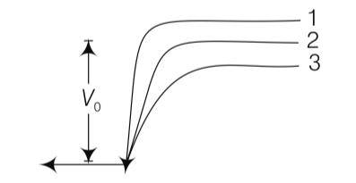
(a) 1 and 3 corresponds to forward bias of junction
(b) 3 corresponds to forward bias of junction and 1 corresponds to reverse bias of the junction
(c) 1 corresponds to forward bias and 3 corresponds to reverse bias of the junction
(d) 3 and 1 both corresponds to reverse bias of the junction
In figure given below V0 is the potential barrier across a pn junction when no battery is connected across the junction

(a) 1 and 3 corresponds to forward bias of junction
(b) 3 corresponds to forward bias of junction and 1 corresponds to reverse bias of the junction
(c) 1 corresponds to forward bias and 3 corresponds to reverse bias of the junction
(d) 3 and 1 both corresponds to reverse bias of the junction
This is a Multiple Choice Questions as classified in NCERT Exemplar
Explanation - When p-n junction is forward biased, it opposes the potential barrier junction, when p-n junction is reverse biased, it supports the potential barrier junction, resulting increase in potential barrier across the ju
Upvote The conductivity of a semiconductor increases with increase in temperature, because
(a) Number density of free current carries increases
(b) Relaxation time increases
(c) Both number density of carries and relaxation time increase
(d) Number density of carries increases, relaxation time decreases but effect of decrease in relaxation time is much less than increase in number density
The conductivity of a semiconductor increases with increase in temperature, because
(a) Number density of free current carries increases
(b) Relaxation time increases
(c) Both number density of carries and relaxation time increase
(d) Number density of carries increases, relaxation time decreases but effect of decrease in relaxation time is much less than increase in number density
This is a Multiple Choice Questions as classified in NCERT Exemplar
Answer- (d)
Explanation- when we increase temperature conductivity increases because number density is increasing after increasing temperature which decreases the relaxation time
Upvote A Zener of power rating 1 W is to be used as a voltage regulator. If Zener has a breakdown of 5 V and it has to regulate voltage which fluctuated between 3 V and 7 V, what should be the value of Rs for safe operation (see figure)?
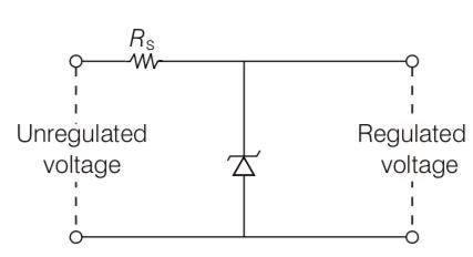
A Zener of power rating 1 W is to be used as a voltage regulator. If Zener has a breakdown of 5 V and it has to regulate voltage which fluctuated between 3 V and 7 V, what should be the value of Rs for safe operation (see figure)?

This is a Short Answer Type Questions as classified in NCERT Exemplar
Explanation- power = 1W
Zener breakdown voltage = 5V
Minimum voltage = 3V
Maximum voltage = 7V
Current = power/voltage= 1/5=0.2A
The value of R for safe operation would be R = max voltage – Zener voltage/current
= 7- 5/0.2 = 2
Upvote Write the truth table for the circuit shown in figure given below. Name the gate that the circuit resembles.
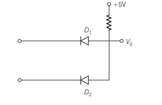
Write the truth table for the circuit shown in figure given below. Name the gate that the circuit resembles.

This is a Short Answer Type Questions as classified in NCERT Exemplar
Explanation- this is AND GATE so truth table for this will be
A | B | A.B |
0 | 0 | |
0 | 1 | 0 |
1 | 0 | 1 |
1 | 1 |
Upvote Explain why elemental semiconductor cannot be used to make visible LEDs.
Explain why elemental semiconductor cannot be used to make visible LEDs.
This is a Short Answer Type Questions as classified in NCERT Exemplar
Explanation- In elemental semiconductor, the band gap is such that the emission are in infrared region and not in visible region.
Upvote