

Semiconductor Electronics
Get insights from 56 questions on Semiconductor Electronics, answered by students, alumni, and experts. You may also ask and answer any question you like about Semiconductor Electronics
Follow Ask QuestionQuestions
Discussions
Active Users
Followers
New answer posted
a year agoContributor-Level 10
For Transistor
to act as a switch → Saturation & cut – off state
to act as an amplifier → Active Region
New answer posted
a year agoContributor-Level 10
This is a Multiple Choice Questions as classified in NCERT Exemplar
Answer- (a, d)
Explanation- In reverse biasing, the minority charge carriers will be accelerated due to reverse biasing, which on striking with atoms cause ionization resulting secondary electrons and thus more number of charge carriers.
When doping concentration is large, there will be large number of ions in the depletion
region, which will give rise to a strong electric field.
New answer posted
a year agoContributor-Level 10
This is a Multiple Choice Questions as classified in NCERT Exemplar
Answer- a, c, d
Explanation-ripple factor is inversely proportional to RL, C and frequency. so to reduce ripple factor all these should be increase.
New answer posted
a year agoContributor-Level 10
This is a Multiple Choice Questions as classified in NCERT Exemplar
Answer-b, d
Explanation- During regulation action of a Zener diode, the current through the Rs changes and resistance offered by the Zener changes. The current through the Zener changes but the voltage across the Zener remains constant.
New answer posted
a year agoContributor-Level 10
This is a Multiple Choice Questions as classified in NCERT Exemplar
Answer- a, b, d
Explanation- The space-charge regions on both the sides of p-n junction which has immobile ions and entirely lacking of any charge carriers will form a region called depletion region of a diode.
The number of ionized acceptors on the p -side equals the number of ionized donors on the n-side.
New answer posted
a year agoContributor-Level 10
This is a Multiple Choice Questions as classified in NCERT Exemplar
Answer- b, c
Explanation- IC= 10mA
Ic= 95/100 Ie
Ie= = 10.53mA
Ib=Ie-IC= 10.53-10= .53mA
New answer posted
a year ago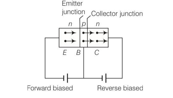
Contributor-Level 10
This is a Multiple Choice Questions as classified in NCERT Exemplar
Answer- a, c
Explanation- Here emitter-base junction is forward biased i.e., the positive pole of emitter base battery is connected to base and its negative pole to emitter. Also, the collector base junction is reverse biased, i.e., the positive pole of the collector base battery is connected to collector and negative pole to base.
Thus, electron move from emmiter to base and cross over from emitter to collector.
New answer posted
a year agoContributor-Level 10
This is a Multiple Choice Questions as classified in NCERT Exemplar
Answer- (a, c)
Explanation- when we apply temperature across semiconductor then electron will starts from lower energy to high energy level that is from valence band to conduction band. When electron goes from lower to higher then holes that is left behind they goes to lower energy levels.
New answer posted
a year ago
Contributor-Level 10
This is a Multiple Choice Questions as classified in NCERT Exemplar
Answer- c
Explanation- C=A.B and D=A'B
E= C+D = (A.B)+ (A'.B)
A | B | A' | C=A.B | D=A'B | E=C+D |
0 | 0 | 1 | 0 | 0 | 0 |
0 | 1 | 1 | 0 | 1 | 1 |
1 | 0 | 0 | 0 | 0 | 0 |
1 | 1 | 0 | 1 | 0 | 1 |
New answer posted
a year ago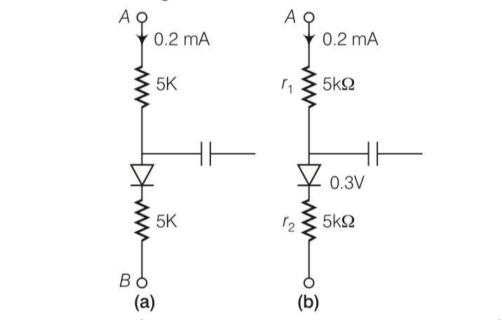
Contributor-Level 10
This is a Multiple Choice Questions as classified in NCERT Exemplar
Answer-b
Explanation- r1=5kohm and r2= 5kohm and both are in series
Then V-0.3 = [ (r1+r2)103] [0.2 10-3]
V-0.3= 2
V= 2.3V
Taking an Exam? Selecting a College?
Get authentic answers from experts, students and alumni that you won't find anywhere else
Sign Up on ShikshaOn Shiksha, get access to
- 66k Colleges
- 1.2k Exams
- 708k Reviews
- 1850k Answers