
Semiconductor Electronics
Get insights from 56 questions on Semiconductor Electronics, answered by students, alumni, and experts. You may also ask and answer any question you like about Semiconductor Electronics
- 56
Questions
- 0
Discussions
- 0
Active Users
- 0
Followers
Have a question about Semiconductor Electronics? Ask our experts
Keep it short & simple. Type complete word. Avoid abusive language.
Why are elemental dopants for Silicon or Germanium usually chosen from group XIII or group XV?
Why are elemental dopants for Silicon or Germanium usually chosen from group XIII or group XV?
This is a Short Answer Type Questions as classified in NCERT Exemplar
Explanation- The size of the dopant atom should be such that their presence in the pure semiconductor does not distort the semiconductor but easily contribute the charge carriers on forming covalent bonds with Si or Ge atoms,
 Upvote

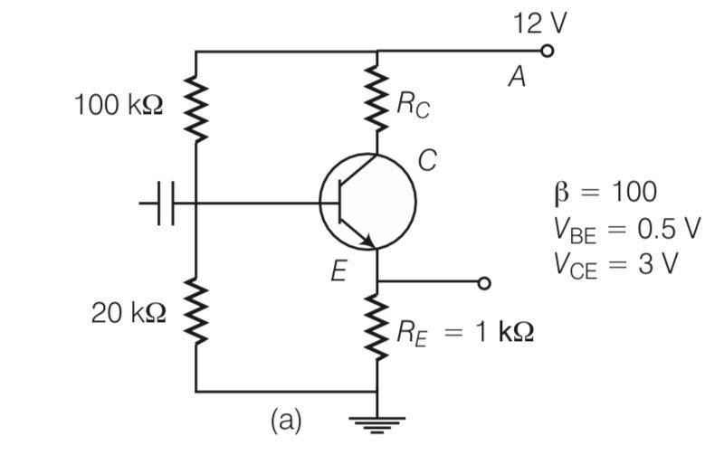
This is a Long Answer Type Questions as classified in NCERT Exemplar
Explanation- IE=IC+IB and Ic=
IcRc+VCE+IERE=VCC
RIB+VBE+IERE=Vcc
IE=Ic=

From above equation
(R+ E)IB=VCC-VBE
IB=
( )=
( )=1.56
Rc=1.56-1=0.56kohm
Upvote For the transistor circuit shown in figure, evaluate VE, RB, RE, given IC= 1 mA, VCE= 3, VBE= 0.5 V and VCC= 12 V, β= 100
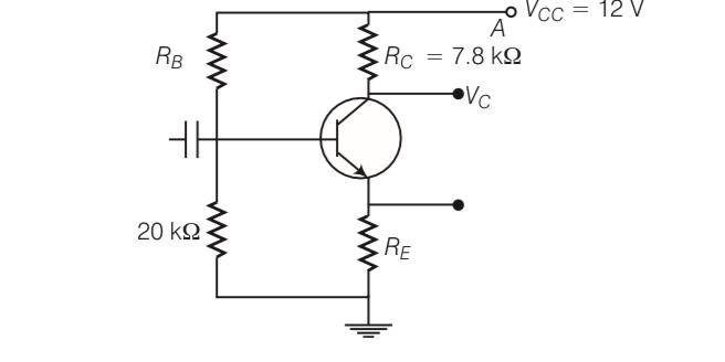
For the transistor circuit shown in figure, evaluate VE, RB, RE, given IC= 1 mA, VCE= 3, VBE= 0.5 V and VCC= 12 V, β= 100
This is a Long Answer Type Questions as classified in NCERT Exemplar
Explanation-Ic= IE
Rc= 7.8Kohm
Ic (Rc+RE)+VCE= 12
(RE+RC)
RE+RC= 9
RE= 9-7.3= 1.2kohm
VE= IE RE
= 1
Voltage VB=VE+VBE= 1.2+0.5= 1.7V
I=
Resistance RB=
 Upvote
Consider a box with three terminals on top of it as shown in figure.
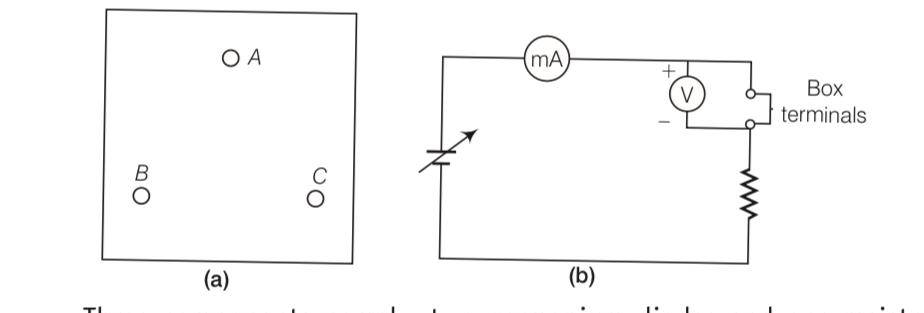
Three components namely, two germanium diodes and one resistor are connected across these three terminals in some arrangement.
A student performs an experiment in which any two of these three terminals are connected in the circuit as shown in figure.
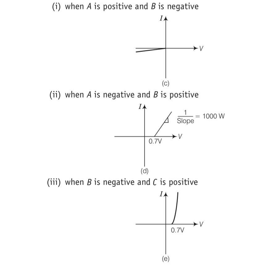
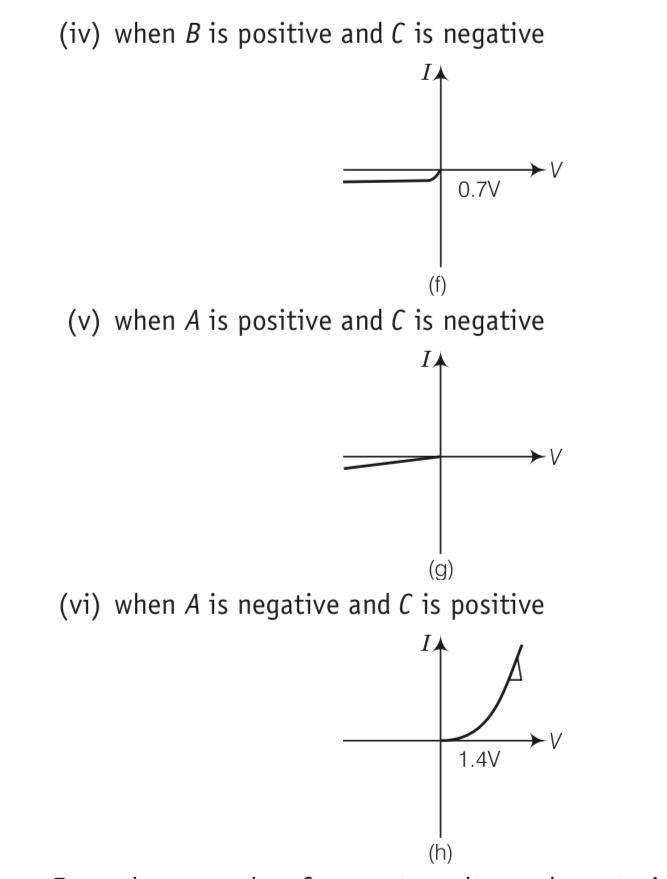
The student obtains graphs of current-voltage characteristics for unknown combination of components between the two terminals connected in the circuit. The graphs are

Three components namely, two germanium diodes and one resistor are connected across these three terminals in some arrangement.
A student performs an experiment in which any two of these three terminals are connected in the circuit as shown in figure.
The student obtains graphs of current-voltage characteristics for unknown combination of components between the two terminals connected in the circuit. The graphs are
This is a Long Answer Type Questions as classified in NCERT Exemplar
Explanation- a) In V- graph of condition (i), a reverse characteristics is shown in fig. (c). Here A is connected to n - side of p-n junction and B is connected to p -side of p-n junction I with a resistance in series.
(b) In V
Upvote An XOR gate has the following truth table. It is represented by following logic relation Y = ? . B + A . B’ . Build this gate using AND, OR and NOT gates
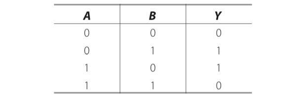
An XOR gate has the following truth table. It is represented by following logic relation Y = ? . B + A . B’ . Build this gate using AND, OR and NOT gates
This is a Long Answer Type Questions as classified in NCERT Exemplar
Y= A'B+A.B'=Y1+Y2
Y1= A.B and Y2= A.B'
Y1 can be obtained as output of AND GATE I for which one Input is of A through NOT GATE and
another input is of B. Y2 can be obtained as output of AND GATE II for which one input is of A
and other
Upvote Suppose a n-type wafer is‘created by doping Si crystal having 5 x 1028atoms/m3 with 1 ppm concentration of As. On the surface 200 ppm boron is added to create ‘p’ region in this wafer. Considering ni = 1.5 x 10¹⁶ m-3,
(i) Calculate the densities of the charge carriers in the n and p regions,
(ii) Comment which charge carriers would contribute largely for the reverse saturation current when diode is reverse biased.
Suppose a n-type wafer is‘created by doping Si crystal having 5 x 1028atoms/m3 with 1 ppm concentration of As. On the surface 200 ppm boron is added to create ‘p’ region in this wafer. Considering ni = 1.5 x 10¹⁶ m-3,
(i) Calculate the densities of the charge carriers in the n and p regions,
(ii) Comment which charge carriers would contribute largely for the reverse saturation current when diode is reverse biased.
This is a Long Answer Type Questions as classified in NCERT Exemplar
whem As is used then it will create n type semiconductor
Ne=ND=
Number of minority carriers nh= = 0.45
But when B is implanted in Si crystal then p type semiconductor is formed
Nh=NA=
Minority carriers created in p type is
Ne=
Mi
Upvote Consider the circuit arrangement shown in Fig 14.16 (a) for studying input and output characteristics of npn transistor in CE configuration
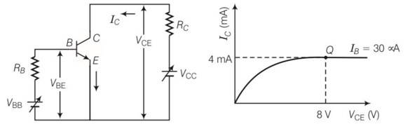
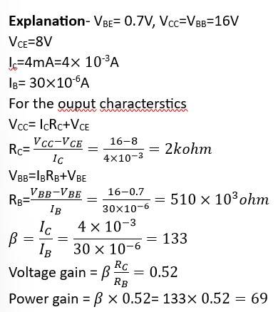
Select the values of RB and RC for a transistor whose VBE = 0.7 V, so that the transistor is operating at point Q as shown in the characteristics shown in Fig. 14.16 (b). Given that the input impedance of the transistor is very small and VCC = VBB = 16 V, also find the voltage gain and power gain of circuit making appropriate assumptions.
Consider the circuit arrangement shown in Fig 14.16 (a) for studying input and output characteristics of npn transistor in CE configuration

Select the values of RB and RC for a transistor whose VBE = 0.7 V, so that the transistor is operating at point Q as shown in the characteristics shown in Fig. 14.16 (b). Given that the input impedance of the transistor is very small and VCC = VBB = 16 V, also find the voltage gain and power gain of circuit making appropriate assumptions.
This is a Long Answer Type Questions as classified in NCERT Exemplar
Upvote Assuming the ideal diode, draw the output waveform for the circuit given in figure, explain the waveform.
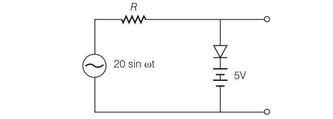
Assuming the ideal diode, draw the output waveform for the circuit given in figure, explain the waveform.

This is a Long Answer Type Questions as classified in NCERT Exemplar
Explanation- When the input voltage is equal to or less than 5 V, diode will be revers biased. It will offer high resistance in comparison to resistance ( ) R in series. Now, diode appears in open circuit. The input waveform is
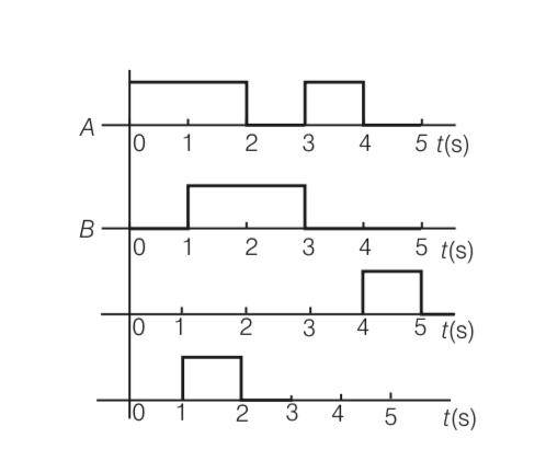
Upvote Draw the output signals C1 and C2 in the given combination of gates.
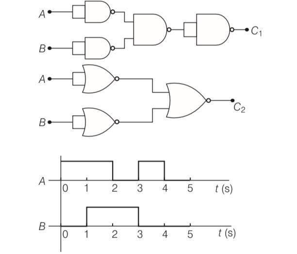
Draw the output signals C1 and C2 in the given combination of gates.

This is a Long Answer Type Questions as classified in NCERT Exemplar
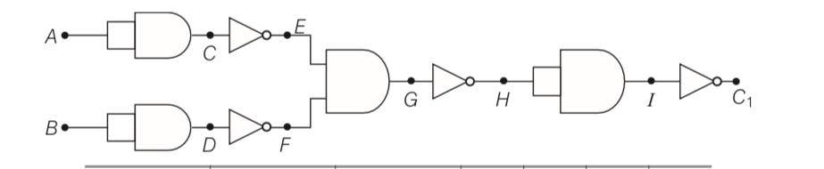
A B | C D | E F | G | H | I | C1 |
0 0 | 0 0 | 1 1 | 1 | 0 | 0 | 1 |
1 0 | 1 0 | 0 1 | 0 | 1 | 1 | 0 |
0 1 | 0 1 | 1 0 | 0 | 1 | 1 | 0 |
1 1 | 1 1 | 0 0 | 0 | 1 | 1 | 0 |
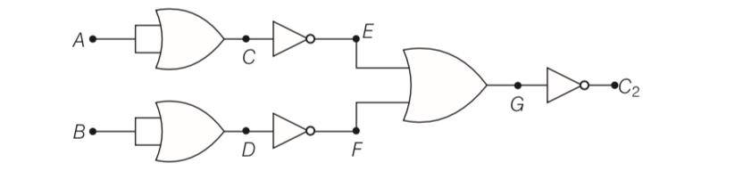
A B | C D | E F | G | C2 |
0 0 | 0 0 | 1 1 | 1 | 0 |
1 0 | 1 0 | 0 1 | 1 | 0 |
0 1 | 0 1 | 1 0 | 1 | 0 |
1 1 | 1 1 | 0 0 | 0 | 1 |
Upvote In the circuit shown in figure, when the input voltage of the base resistance is 10 V, VBEis zero and VCE is also zero. Find the values of IB, IC and β .
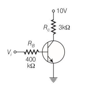
In the circuit shown in figure, when the input voltage of the base resistance is 10 V, VBEis zero and VCE is also zero. Find the values of IB, IC and β .

This is a Long Answer Type Questions as classified in NCERT Exemplar
Explanation- voltage across RB= 10V
Resistance RB= 400kohm
VBE= 0, VCE= 0, Rc=3kohm
IB= voltage /RB= 10/400 103= 25 10-6A
Voltage across Rc= 10V
Ic=voltage/Rc= 10/3 103= 3.33 10-3
Upvote