

Physics
Get insights from 5.6k questions on Physics, answered by students, alumni, and experts. You may also ask and answer any question you like about Physics
Follow Ask QuestionQuestions
Discussions
Active Users
Followers
New answer posted
a year ago
Contributor-Level 10
Explanation- mass of earth M = 6
Radius of the earth , R = 6400km= 6.4
T=24h= 24
G = 6.67 10-11Nm2/kg2
(a) Time period T =
= 2
= ( )1/3
( )1/3-R
So after solving we get h = 3.59
(b) If satellite is at height h from the earth's surface

Cos = = cos81018'
= 81018'
=2(81018')= 162036'
If n number of satellite needed to cover entire the earth then
So n = 3600/2 = 2.31
So minimum 3 satellite are required to cover entire earth.
New answer posted
a year agoContributor-Level 10
This is a Long Type Questions as classified in NCERT Exemplar
Explanation- consider a diagram having vertices A,B,C,D,E and F

AC= AG+GC=2AG
= 2lcos300= 2l
=
AD=AH+HJ+JD= lsin300+l+lsin300=2l
Force on mass m at A due to mass m at B is f1= along AB
Force on mass m at A due to mass m at C is f2= along AC
Force on mass m at A due to mass m at D is F3= along AD
Force on mass m at A due to mass m at E is F4= = along AE
Force on mass m at A due to mass m at F is F5= along AF
Resultant force due to F1 and F5 is F1=
= along AD
So net force along AD = F1+F2+F3=
New answer posted
a year agoContributor-Level 10
This is a Long Type Questions as classified in NCERT Exemplar
Explanation- when a body og mass m is revolving around a star of mass M.
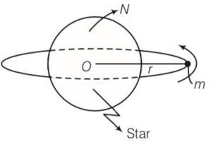
Linear velocity of the body v= so when r increases then v decreases.
Angular velocity of the body w = 2
According to kepler's law T2 r3
So T= kr3/2
So w= so when r increases, w decreases.
Kinetic energy of the body K= 1/2mv2=1/2m ( ) so when we increase r, KE decreases.
Gravitational potential energy of the body
U=-GMm/r
So when we increase r, PE becomes less negative
Total energy of the body E= KE+PE=
When r increases total energy becomes less negative . i.e increases.
Angular mom
New answer posted
a year agoContributor-Level 10
For numerical problems, start by finding the given data and know what needs to be calculated. To visualize the motion, it is advisable to use a diagram. Based on if the acceleration is uniform, choose the appropriate kinematic equations. Also, be careful with the unit conversions and sign conventions. Solve the numerical problems by following the step-by-step approach and at the end double-check your answer for accuracy.
New answer posted
a year agoContributor-Level 10
Yes, if one practices from the NCERT Exemplar, they can score high in the CBSE Board exams and entrance exams like NEET and JEE. The exemplar questions include advanced and application-based questions which deepen students' understanding of key concepts. It contains information beyond the NCERT textbook and offers concept clarity to students. Practicing from the exemplar helps in improving the problem-solving skills of the students.
New answer posted
a year agoContributor-Level 10
Motion in a Straight Line focuses on the rectilinear motion, which is the motion of objects along a single straight path. It covers key concepts such as speed, displacement, acceleration, velocity, and motion graphs. It helps students understand more complex types of motions.
New answer posted
a year agoContributor-Level 10
If one solves all these questions then it is great but it is not something mandatory. Practicing these questions helps students develop a strong understanding of Coulomb's law, electric charges, the superposition principle, and electric field lines. Even practicing a significant portion helps in boosting exam confidence and helps students to score high in the examination.
New answer posted
a year agoContributor-Level 10
The NCERT textbook is good to start with as it introduces students to the basic concepts and explains these topics to provide conceptual clarity. However, the exemplar focuses on reasoning, challenging multiple-choice questions and numerical problems. The exemplar is like the supplement that boosts students' grasp on these concepts given in the NCERT textbook through reasoning, multiple-choice and numerical problems.
New answer posted
a year agoContributor-Level 10
Chapter 1 Electric Charges and Fields NCERT Exemplar goes beyond the basic NCERT textbook and contains application-based and advanced-level questions. It is designed to enhance students' problem-solving skills, improve their understanding of electrostatics, and prepare them for their CBSE board exams and competitive exams like NEET and JEE.
New answer posted
a year agoContributor-Level 10
This is a Multiple Choice Questions as classified in NCERT Exemplar
Answer- (a, d)
Explanation- In reverse biasing, the minority charge carriers will be accelerated due to reverse biasing, which on striking with atoms cause ionization resulting secondary electrons and thus more number of charge carriers.
When doping concentration is large, there will be large number of ions in the depletion
region, which will give rise to a strong electric field.
Taking an Exam? Selecting a College?
Get authentic answers from experts, students and alumni that you won't find anywhere else
Sign Up on ShikshaOn Shiksha, get access to
- 66k Colleges
- 1.2k Exams
- 705k Reviews
- 1850k Answers