 / Preparation Physics NCERT Exemplar Solutions Class 12th Chapter Fourteen
- Semiconductor Electronics Long Answer Type Questions
- Chapters List
- Semiconductor Electronics More Long Answer Type Questions
- Semiconductor Electronics Short Answer Type Questions
- Semiconductor Electronics Multiple Choice Questions
Semiconductor Electronics Long Answer Type Questions
| 1. If each diode in figure has a forward bias resistance of 25 Ω and infinite resistance in reverse bias, what will be the values of the currents I1, I2, I3and I4? 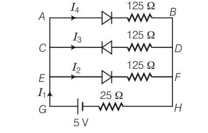
|
| Explanation- forward biased resistance = 25ohm Reverse biased resistance = infinity As CD branch is reverse biased having infinite resistance. So I3= 0 Resistance in branch AB= 25+125= 150 ohm(R1) Resistance in branch EF= 25+125= 150 ohm(R2) They both are in parallel So R= 75ohm So total resistance = 25+75= 100ohm Current = V/R= 5/100=0.05A I1=I2+I3+I4 I1=I4+I2 Here the resistance R1 and R2 is same I4=I2 I1= 2I2 I2= I1/2=0.05/2=0.025A I4= 0.025A |
| 2. In the circuit shown in figure, when the input voltage of the base resistance is 10 V, VBEis zero and VCE is also zero. Find the values of IB, IC and β . 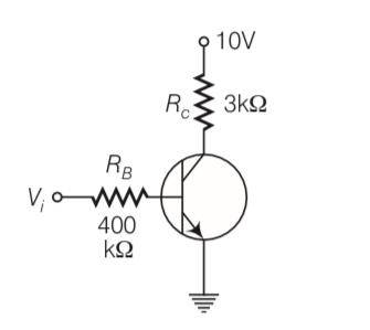
|
| Explanation- voltage across RB= 10V Resistance RB= 400kohm VBE= 0, VCE= 0 , Rc=3kohm IB= voltage /RB= 10/400 103= 25 10-6A Voltage across Rc= 10V Ic=voltage/Rc= 10/3 103= 3.33 10-3
|
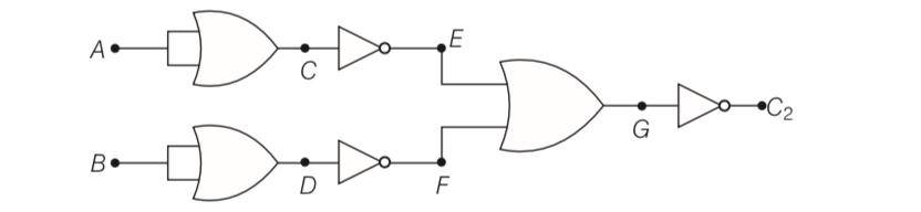
| 3. Draw the output signals C1 and C2 in the given combination of gates. 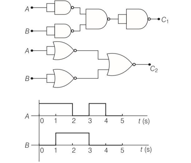
|
||||||||||||||||||||||||||||||||||||||||||||||||||||||||||||
| Explanation- 
|
| 4. Assuming the ideal diode, draw the output waveform for the circuit given in figure, explain the waveform. 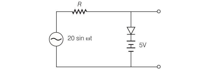
|
| Explanation- When the input voltage is equal to or less than 5 V, diode will be revers biased. It will offer high resistance in comparison to resistance ( ) R in series. Now, diode appears in open circuit. The input waveform is then passed to the output terminals. The result with sin wave input is to dip off all positive going portion above 5 V. If input voltage is more than + 5 V, diode will be conducting as if forward biased offering low resistance in comparison to R. But there will be no voltage in output beyond 5 V as the voltagebeyond+5Vwillappearacross R. When input voltage is negative, there will be opposition to 5 V battery in p n- junction input voltage becomes more than− 5 V, the diode will be reverse biased. It will offer high resistance in comparison to resistance R in series. Now junction diode appears in open circuit. The input waveform is then passed on to the output terminals. The output waveform is shown here in the fig. (b) 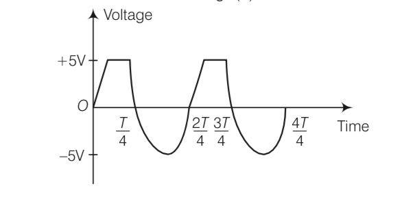
|

Commonly asked questions
Assuming the ideal diode, draw the output waveform for the circuit given in figure, explain the waveform.

This is a Long Answer Type Questions as classified in NCERT Exemplar
Explanation- When the input voltage is equal to or less than 5 V, diode will be revers biased. It will offer high resistance in comparison to resistance ( ) R in series. Now, diode appears in open circuit. The input waveform is then passed to the output terminals. The result with sin wave input is to dip off all positive going portion above 5 V.
If input voltage is more than + 5 V, diode will be conducting as if forward biased offering low resistance in comparison to R. But there will be no voltage in output beyond 5 V as the
voltagebeyond+5Vwillappearacross R.
When input voltage is negative, there will be opposition to 5 V battery in p n- junction input voltage becomes more than? 5 V, the diode will be reverse biased. It will offer high resistance in comparison to resistance R in series. Now junction diode appears in open circuit. The input waveform is then passed on to the output terminals.
The output waveform is shown here in the fig. (b)

The breakdown in a reverse biased p-n junction is more likely to occur due to
(a) Large velocity of the minority charge carriers if the doping concentration is small
(b) Large velocity of the minority charge carriers if the doping concentration is large
(c) Strongelectricfieldinadepletionregionifthedopingconcentrationissmall
(d) Strong electric field in the depletion region if the doping concentration is large
This is a Multiple Choice Questions as classified in NCERT Exemplar
Answer- (a, d)
Explanation- In reverse biasing, the minority charge carriers will be accelerated due to reverse biasing, which on striking with atoms cause ionization resulting secondary electrons and thus more number of charge carriers.
When doping concentration is large, there will be large number of ions in the depletion
region, which will give rise to a strong electric field.
If each diode in figure has a forward bias resistance of 25 Ω and infinite resistance in reverse bias, what will be the values of the currents I1, I2, I3and I4?
This is a Long Answer Type Questions as classified in NCERT Exemplar
forward biased resistance = 25ohm
Reverse biased resistance = infinity
As CD branch is reverse biased having infinite resistance.
So I3= 0
Resistance in branch AB= 25+125= 150 ohm (R1)
Resistance in branch EF= 25+125= 150 ohm (R2)
They both are in parallel
So
R= 75ohm
So total resistance = 25+75= 100ohm
Current = V/R= 5/100=0.05A
I1=I2+I3+I4
I1=I4+I2
Here the resistance R1 and R2 is same
I4=I2
I1= 2I2
I2= I1/2=0.05/2=0.025A
I4= 0.025A
In the circuit shown in figure, when the input voltage of the base resistance is 10 V, VBEis zero and VCE is also zero. Find the values of IB, IC and β .

This is a Long Answer Type Questions as classified in NCERT Exemplar
Explanation- voltage across RB= 10V
Resistance RB= 400kohm
VBE= 0, VCE= 0, Rc=3kohm
IB= voltage /RB= 10/400 103= 25 10-6A
Voltage across Rc= 10V
Ic=voltage/Rc= 10/3 103= 3.33 10-3
Draw the output signals C1 and C2 in the given combination of gates.

This is a Long Answer Type Questions as classified in NCERT Exemplar
A B | C D | E F | G | H | I | C1 |
0 0 | 0 0 | 1 1 | 1 | 0 | 0 | 1 |
1 0 | 1 0 | 0 1 | 0 | 1 | 1 | 0 |
0 1 | 0 1 | 1 0 | 0 | 1 | 1 | 0 |
1 1 | 1 1 | 0 0 | 0 | 1 | 1 | 0 |
A B | C D | E F | G | C2 |
0 0 | 0 0 | 1 1 | 1 | 0 |
1 0 | 1 0 | 0 1 | 1 | 0 |
0 1 | 0 1 | 1 0 | 1 | 0 |
1 1 | 1 1 | 0 0 | 0 | 1 |
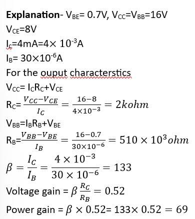
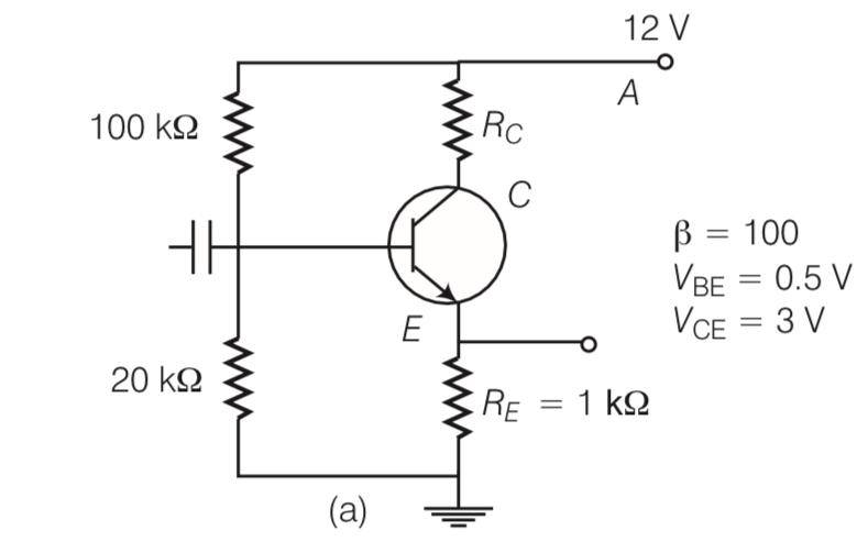
Consider the circuit arrangement shown in Fig 14.16 (a) for studying input and output characteristics of npn transistor in CE configuration

Select the values of RB and RC for a transistor whose VBE = 0.7 V, so that the transistor is operating at point Q as shown in the characteristics shown in Fig. 14.16 (b). Given that the input impedance of the transistor is very small and VCC = VBB = 16 V, also find the voltage gain and power gain of circuit making appropriate assumptions.
This is a Long Answer Type Questions as classified in NCERT Exemplar
Suppose a n-type wafer is‘created by doping Si crystal having 5 x 1028atoms/m3 with 1 ppm concentration of As. On the surface 200 ppm boron is added to create ‘p’ region in this wafer. Considering ni = 1.5 x 10¹⁶ m-3,
(i) Calculate the densities of the charge carriers in the n and p regions,
(ii) Comment which charge carriers would contribute largely for the reverse saturation current when diode is reverse biased.
This is a Long Answer Type Questions as classified in NCERT Exemplar
whem As is used then it will create n type semiconductor
Ne=ND=
Number of minority carriers nh= = 0.45
But when B is implanted in Si crystal then p type semiconductor is formed
Nh=NA=
Minority carriers created in p type is
Ne=
Minority charge carriers holes in p type would contribute more in reverse saturatiom current.
An XOR gate has the following truth table. It is represented by following logic relation Y = ? . B + A . B’ . Build this gate using AND, OR and NOT gates
This is a Long Answer Type Questions as classified in NCERT Exemplar
Y= A'B+A.B'=Y1+Y2
Y1= A.B and Y2= A.B'
Y1 can be obtained as output of AND GATE I for which one Input is of A through NOT GATE and
another input is of B. Y2 can be obtained as output of AND GATE II for which one input is of A
and other input is of B through NOT gate.
Now Y2 can be obtained as output from or gate, where, Y1 and Y2 are input of or gate.
Thus, the given table can be obtained from the logic circuit given below


Three components namely, two germanium diodes and one resistor are connected across these three terminals in some arrangement.
A student performs an experiment in which any two of these three terminals are connected in the circuit as shown in figure.
The student obtains graphs of current-voltage characteristics for unknown combination of components between the two terminals connected in the circuit. The graphs are
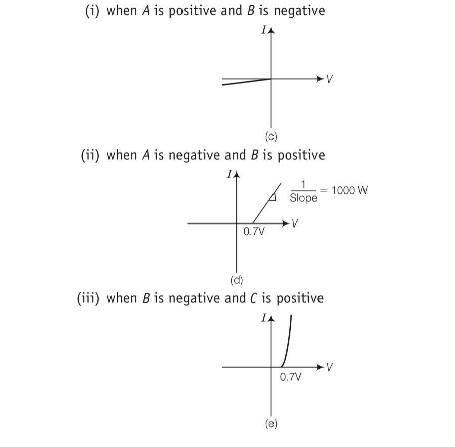
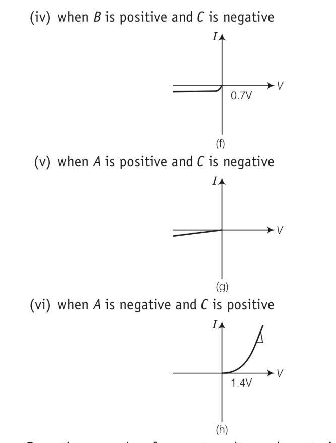
This is a Long Answer Type Questions as classified in NCERT Exemplar
Explanation- a) In V- graph of condition (i), a reverse characteristics is shown in fig. (c). Here A is connected to n - side of p-n junction and B is connected to p -side of p-n junction I with a resistance in series.
(b) In V- graph of condition (ii), a forward characteristics is shown in fig. (d), where 0.7 V is
the knee voltage of p-n junction I 1/slope= (1/1000)? It means A is connected to n -side of p n- junction and B is connected to p-side of p n- junction and resistance R is in series of p n- junction between A and B.
(c) In V- graph of condition (iii), a forward characteristics is shown in figure (e), where 0.7 V is the knee voltage. In this case p -side of p-n junction II is connected to C and n -side of p-n junction II to B.

(d) In V-I graphs of conditions (iv), (v), (vi) also concludes the above connection of p-n junctions I and II along with a resistance R.
Thus, the arrangement of p-n I, p-n II and resistance R between A B, in the figure p-n I, p-n II and C will be as shown.
For the transistor circuit shown in figure, evaluate VE, RB, RE, given IC= 1 mA, VCE= 3, VBE= 0.5 V and VCC= 12 V, β= 100
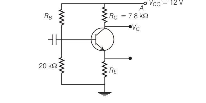
This is a Long Answer Type Questions as classified in NCERT Exemplar
Explanation-Ic= IE
Rc= 7.8Kohm
Ic (Rc+RE)+VCE= 12
(RE+RC)
RE+RC= 9
RE= 9-7.3= 1.2kohm
VE= IE RE
= 1
Voltage VB=VE+VBE= 1.2+0.5= 1.7V
I=
Resistance RB=

In the circuit diagram find the value of Rc
This is a Long Answer Type Questions as classified in NCERT Exemplar
Explanation- IE=IC+IB and Ic=
IcRc+VCE+IERE=VCC
RIB+VBE+IERE=Vcc
IE=Ic=

From above equation
(R+ E)IB=VCC-VBE
IB=
( )=
( )=1.56
Rc=1.56-1=0.56kohm
Why are elemental dopants for Silicon or Germanium usually chosen from group XIII or group XV?
This is a Short Answer Type Questions as classified in NCERT Exemplar
Explanation- The size of the dopant atom should be such that their presence in the pure semiconductor does not distort the semiconductor but easily contribute the charge carriers on forming covalent bonds with Si or Ge atoms, which are provided by group XIII or group XV elements.
Sn, C and Si, Ge are all group XIV elements. Yet, Sn is a conductor, C is an insulator while Si and Ge are semiconductors. Why?
This is a Short Answer Type Questions as classified in NCERT Exemplar
Explanation- A material is a conductor if in its energy band diagram, there is no energy gap between conduction band and valence band. For insulator, the energy gap is large and for
semiconductor the energy gap is moderate.
The energy gap for Sn is 0 eV, for C is 5.4 eV, for Si is 1.1 eV and for Ge is 0.7 eV, related to their atomic size. Therefore Sn is a conductor, C is an insulator and Ge and Si are semiconductors.
Can the potential barrier across a p-n junction be measured by simply connecting a voltmeter across the junction?
This is a Short Answer Type Questions as classified in NCERT Exemplar
Explanation- We cannot measure the potential barrier across a p-n junction by a voltmeter because the resistance of voltmeter is very high as compared to the junction resistance.
Draw the output waveform across the resistor in the given figure.

This is a Short Answer Type Questions as classified in NCERT Exemplar
Explanation- diode only works in forward biased. So output waveform is

The amplifiers X, Y and Z are connected in series. If the voltage gains of X, Y and Z are 10,20 and 30, respectively and the input signal is 1 mV peak value, then what is the output signal voltage (peak value).
(i) If DC supply voltage is 10 V?
(ii) If DC supply voltage is 5 V?
This is a Short Answer Type Questions as classified in NCERT Exemplar
Explanation- as we know total voltage amplification =
Avx= 10, Avy = 20, Avz = 30
vi = 1mV= 10-3V
So according to formula
= (Avx ) (Avy ) (Avz)
vo = (Avx ) (Avy ) (Avz) vi
= 10-3 =6V
So in first case output cannot be greater than 6V but in 2nd case it will work
In a CE transistor amplifier, there is a current and voltage gain associated with the circuit. In other words there is a power gain. Considering power a measure of energy, does the circuit violate conservation of energy?
This is a Short Answer Type Questions as classified in NCERT Exemplar
Explanation- In CE transistor amplifier, the power gain is very high.
In this circuit, the extra power required for amplified output is obtained from DC source.
Thus, the circuit used does not violet the law of conservation.
(i) Name the type of a diode whose characteristics are shown in figure (a) and (b).
(ii) What does the point P in fig. (a) represent?
(iii) What does the points P and Q in fig. (b) represent?
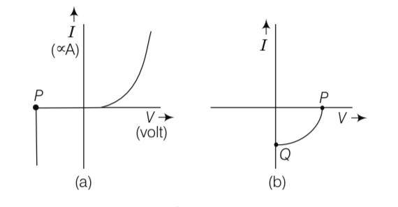
This is a Short Answer Type Questions as classified in NCERT Exemplar
Explanation- (i) The characteristic curve (a) is of Zener diode and curve (b) is of solar cell.
(ii) The point P in fig. (a) represents Zener break down voltage.
(iii) In fig. (b), the point Q represents zero voltage and negative current. It means light falling on solar cell with atleast minimum threshold frequency gives the current in opposite direction to that due to a battery connected to solar cell. But for the point Q, the battery is short circuited. Hence represents the short circuit current.
In fig. (b), the point P represents some positive voltage on solar cell with zero current
Through solar cell.It means, there is a battery connected to a solar cell which gives rise to the equal and Opposite current to that in solar cell by virtue of light falling on it.
As current is zero for point P, hence we say P represents open circuit voltage.
Three photo diodes D1, D2and D3 are made of semiconductors having band gaps of 2.5 eV, 2 eV and 3 eV, respectively. Which ones will be able to detect light of wavelength 6000 Å ?
This is a Short Answer Type Questions as classified in NCERT Exemplar
Explanation- E=hc/ = = 2.06eV
The incident radiation which is detected by the photodiode having energy should be greater
Than the band-gap. So, it is only valid for diode D2.Then, diode D2 will detect this radiation.
If the resistance R1is increased (see figure), how will the readings of the ammeter and voltmeter change?

This is a Short Answer Type Questions as classified in NCERT Exemplar
Explanation- as base current IB =
As Ri is increased IB is decreased.

And collector current is Ic = IB as IB decreased Ic also decreased and the rading of voltmeter and ammeter also decreased.
Two car garages have a common gate which needs to open automatically when a car enters either of the garages or cars enter both. Draw a circuit that resembles this situation using diodes for this situation.

This is a Short Answer Type Questions as classified in NCERT Exemplar
Explanation-
OR GATE gives the desired output.
A | B | C |
0 | 0 | |
0 | 1 | 1 |
1 | 0 | 1 |
1 | 1 |
How would you set up a circuit to obtain NOT gate using a transistor?
This is a Short Answer Type Questions as classified in NCERT Exemplar
Explanation- The NOT GATE is a device which has only one input and one output i.e., A'=Y means Y equals NOT A.

This GATE cannot be realised by using diodes. However it can be realised by making use of a
transistor. This can be seen in the figure given below.
A | Y |
0 | 1 |
1 | 0 |
Here, the base B of the transistor is connected to the input A through a resistance Rb and the emitter E is earthed. The collector is connected to 5 V battery. The output Y is the voltage at C w.r.t. earth.
The resistor Rb and Rc are so chosen that if emitter-base junction is unbiased, the transistor is in cut off mode and if emitter-base junction is forward biased by 5V, the transistor is in saturation state.
Explain why elemental semiconductor cannot be used to make visible LEDs.
This is a Short Answer Type Questions as classified in NCERT Exemplar
Explanation- In elemental semiconductor, the band gap is such that the emission are in infrared region and not in visible region.
Write the truth table for the circuit shown in figure given below. Name the gate that the circuit resembles.

This is a Short Answer Type Questions as classified in NCERT Exemplar
Explanation- this is AND GATE so truth table for this will be
A | B | A.B |
0 | 0 | |
0 | 1 | 0 |
1 | 0 | 1 |
1 | 1 |
A Zener of power rating 1 W is to be used as a voltage regulator. If Zener has a breakdown of 5 V and it has to regulate voltage which fluctuated between 3 V and 7 V, what should be the value of Rs for safe operation (see figure)?

This is a Short Answer Type Questions as classified in NCERT Exemplar
Explanation- power = 1W
Zener breakdown voltage = 5V
Minimum voltage = 3V
Maximum voltage = 7V
Current = power/voltage= 1/5=0.2A
The value of R for safe operation would be R = max voltage – Zener voltage/current
= 7- 5/0.2 = 2/0.2 = 10ohm
The conductivity of a semiconductor increases with increase in temperature, because
(a) Number density of free current carries increases
(b) Relaxation time increases
(c) Both number density of carries and relaxation time increase
(d) Number density of carries increases, relaxation time decreases but effect of decrease in relaxation time is much less than increase in number density
This is a Multiple Choice Questions as classified in NCERT Exemplar
Answer- (d)
Explanation- when we increase temperature conductivity increases because number density is increasing after increasing temperature which decreases the relaxation time
In figure given below V0 is the potential barrier across a pn junction when no battery is connected across the junction

(a) 1 and 3 corresponds to forward bias of junction
(b) 3 corresponds to forward bias of junction and 1 corresponds to reverse bias of the junction
(c) 1 corresponds to forward bias and 3 corresponds to reverse bias of the junction
(d) 3 and 1 both corresponds to reverse bias of the junction
This is a Multiple Choice Questions as classified in NCERT Exemplar
Explanation - When p-n junction is forward biased, it opposes the potential barrier junction, when p-n junction is reverse biased, it supports the potential barrier junction, resulting increase in potential barrier across the junction.
In figure given on next page, assuming the diodes to be ideal
(a) D1is forward biased and D2 is reverse biased and hence current flows from A to B
(b) D2 is forward biased and D1 is reverse biased and hence no current flows from B to A and vice-versa
(c) D1 and D2 are both forward biased and hence current flows from A to B
(d) D1 and D2 are both reverse biased and hence no current flows from A to B and vice-versa

This is a Multiple Choice Questions as classified in NCERT Exemplar
Answer-b
Explanation- from the figure we can say that diode D1 is reverse biased and diode D2 is forward biased so current will flow from B to A.
A 220 V AC supply is connected between points A and B (figure). What will be the potential difference V across the capacitor?

This is a Multiple Choice Questions as classified in NCERT Exemplar
Answer- d
Explanation- as we know that Ev = Eo/ so E0= Ev so net voltage is 220 V
Hole is
(a) An anti-particle of electron
(b) A vacancy created when an electron leaves a covalent bond
(c) Absence of free electrons
(d) An artificially created particle
This is a Multiple Choice Questions as classified in NCERT Exemplar
Answer-b
Explanation -when a neutral entity is there it contains both equal number of elctron and holes. Also when electron emit from neutral entity then it leave behind a vacancy that is hole.
The output of the given circuit in figure is given below.

(c) Would be like a half wave rectifier with negative cycles in output
(d) Would be like that of a full wave rectifier
This is a Multiple Choice Questions as classified in NCERT Exemplar
Answer- c
Explanation- due to forward biasing the diffusion current in the circuit is very high and resistance in the circuit is very low. Thus voltage across pn junction is very low but in case of reverse biasing diffusion current very small so resistance becomes very high . and that end making high voltage across pn junction.
In the circuit shown in figure given below, if the diode forward voltage between A and B is
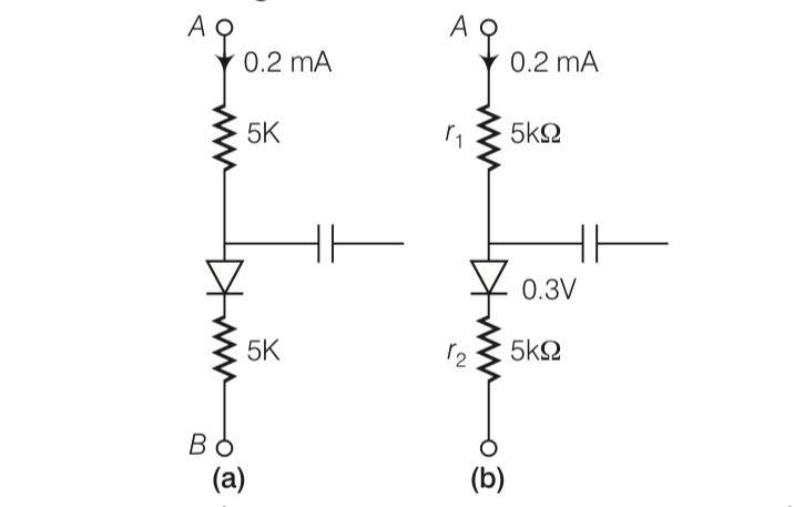
This is a Multiple Choice Questions as classified in NCERT Exemplar
Answer-b
Explanation- r1=5kohm and r2= 5kohm and both are in series
Then V-0.3 = [ (r1+r2)103] [0.2 10-3]
V-0.3= 2
V= 2.3V
Truth table for the given circuit is

This is a Multiple Choice Questions as classified in NCERT Exemplar
Answer- c
Explanation- C=A.B and D=A'B
E= C+D = (A.B)+ (A'.B)
A | B | A' | C=A.B | D=A'B | E=C+D |
0 | 0 | 1 | 0 | 0 | 0 |
0 | 1 | 1 | 0 | 1 | 1 |
1 | 0 | 0 | 0 | 0 | 0 |
1 | 1 | 0 | 1 | 0 | 1 |
When an electric field is applied across a semiconductor
(a) Electrons move from lower energy level to higher energy level in the conduction band
(b) Electrons move from higher energy level to lower energy level in the conduction band
(c) Holes in the valence band move from higher energy level to lower energy level
(d) Holes in the valence band move from lower energy level to higher energy level
This is a Multiple Choice Questions as classified in NCERT Exemplar
Answer- (a, c)
Explanation- when we apply temperature across semiconductor then electron will starts from lower energy to high energy level that is from valence band to conduction band. When electron goes from lower to higher then holes that is left behind they goes to lower energy levels.
Consider an n-p-n transistor with its base-emitter junction forward biased and collector base junction reverse biased. Which of the following statements are true?
(a) Electrons crossover from emitter to collector
(b) Holes move from base to collector
(c) Electrons move from emitter to base
(d) Electrons from emitter move out of base without going to the collector
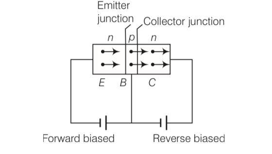
This is a Multiple Choice Questions as classified in NCERT Exemplar
Answer- a, c
Explanation- Here emitter-base junction is forward biased i.e., the positive pole of emitter base battery is connected to base and its negative pole to emitter. Also, the collector base junction is reverse biased, i.e., the positive pole of the collector base battery is connected to collector and negative pole to base.
Thus, electron move from emmiter to base and cross over from emitter to collector.
In a n-p-n transistor circuit, the collector current is 10 mA. If 95 per cent of the electrons emitted reach the collector, which of the following statements are true?
(a) The emitter current will be 8 mA
(b) The emitter current will be 10.53 mA
(c) The base current will be 0.53 mA
(d) The base current will be 2 mA
This is a Multiple Choice Questions as classified in NCERT Exemplar
Answer- b, c
Explanation- IC= 10mA
Ic= 95/100 Ie
Ie= = 10.53mA
Ib=Ie-IC= 10.53-10= .53mA
In the depletion region of a diode
(a) There are no mobile charges
(b) Equal number of holes and elections exist, making the region neutral
(c) Recombination of holes and electrons has taken place
(d) Immobile charged ions exist
This is a Multiple Choice Questions as classified in NCERT Exemplar
Answer- a, b, d
Explanation- The space-charge regions on both the sides of p-n junction which has immobile ions and entirely lacking of any charge carriers will form a region called depletion region of a diode.
The number of ionized acceptors on the p -side equals the number of ionized donors on the n-side.
What happens during regulation action of a Zener diode?
(a) The current and voltage across the Zener remains fixed
(b) The current through the series Resistance (Rs) changes
(c) The Zener resistance is constant
(d) The resistance offered by the Zener changes
This is a Multiple Choice Questions as classified in NCERT Exemplar
Answer-b, d
Explanation- During regulation action of a Zener diode, the current through the Rs changes and resistance offered by the Zener changes. The current through the Zener changes but the voltage across the Zener remains constant.
To reduce the ripples in rectifier circuit with capacitor filter
(a) RLshould be increased
(b) Input frequency should be decreased .
(c) Input frequency should be increased
(d) Capacitors with high capacitance should be used
This is a Multiple Choice Questions as classified in NCERT Exemplar
Answer- a, c, d
Explanation-ripple factor is inversely proportional to RL, C and frequency. so to reduce ripple factor all these should be increase.
Chapters List
Semiconductor Electronics More Long Answer Type Questions
| 5. Consider the circuit arrangement shown in Fig 14.16 (a) for studying input and output characteristics of npn transistor in CE configuration 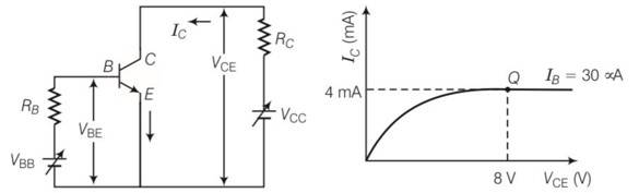
Select the values of RB and RC for a transistor whose VBE = 0.7 V, so that the transistor is operating at point Q as shown in the characteristics shown in Fig. 14.16 (b). Given that the input impedance of the transistor is very small and VCC = VBB = 16 V, also find the voltage gain and power gain of circuit making appropriate assumptions. |
|
|
| 6. Suppose a n-type wafer is‘created by doping Si crystal having 5 x 1028atoms/m3 with 1 ppm concentration of As. On the surface 200 ppm boron is added to create ‘p’ region in this wafer. Considering ni = 1.5 x 10¹⁶ m-3, |
| Explanation- whem As is used then it will create n type semiconductor Ne=ND= Number of minority carriers nh= = 0.45 But when B is implanted in Si crystal then p type semiconductor is formed Nh=NA= Minority carriers created in p type is Ne= Minority charge carriers holes in p type would contribute more in reverse saturatiom current. |
| 7. An XOR gate has the following truth table. It is represented by following logic relation Y = Ᾱ . B + A . B’ . Build this gate using AND, OR and NOT gates
|
| Explanation- Y= A’B+A.B’=Y1+Y2 Y1= A.B and Y2= A.B’ Y1 can be obtained as output of AND gate I for which one Input is of A through NOT gate and another input is of B. Y2 can be obtained as output of AND gate II for which one input is of A and other input is of B through NOT gate. Now Y2 can be obtained as output from OR gate, where, Y1 and Y2 are input of OR gate. Thus, the given table can be obtained from the logic circuit given below 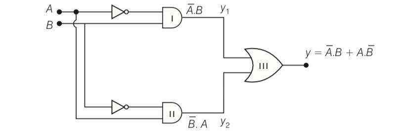
|
| 8. Consider a box with three terminals on top of it as shown in figure. 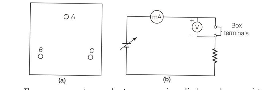
Three components namely, two germanium diodes and one resistor are connected across these three terminals in some arrangement.
|
| Explanation- a) In V- graph of condition (i), a reverse characteristics is shown in fig. (c). Here A is connected to n - side of p-n junction and B is connected to p -side of p-n junction I with a resistance in series. (b) In V- graph of condition (ii), a forward characteristics is shown in fig. (d), where 0.7 V is the knee voltage of p-n junction I 1/slope= (1/1000) Ω. It means A is connected to n -side of p n- junction and B is connected to p-side of p n- junction and resistance R is in series of p n- junction between A and B. (c) In V- graph of condition (iii), a forward characteristics is shown in figure (e), where 0.7 V is the knee voltage. In this case p -side of p-n junction II is connected to C and n -side of p-n junction II to B. 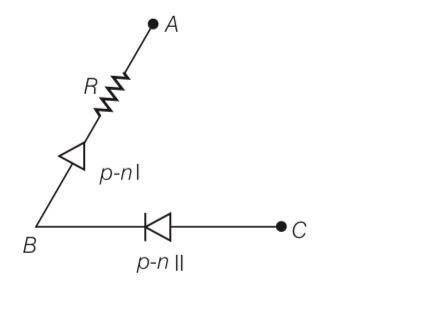
(d) In V-I graphs of conditions (iv), (v), (vi) also concludes the above connection of p-n junctions I and II along with a resistance R. |
| 9. For the transistor circuit shown in figure, evaluate VE, RB, RE, given IC= 1 mA, VCE= 3, VBE= 0.5 V and VCC= 12 V, β= 100
|
| Explanation-Ic= IE Rc= 7.8Kohm Ic(Rc+RE)+VCE= 12 (RE+RC) RE+RC= 9 RE= 9-7.3= 1.2kohm VE= IE RE = 1 Voltage VB=VE+VBE= 1.2+0.5= 1.7V I= Resistance RB= 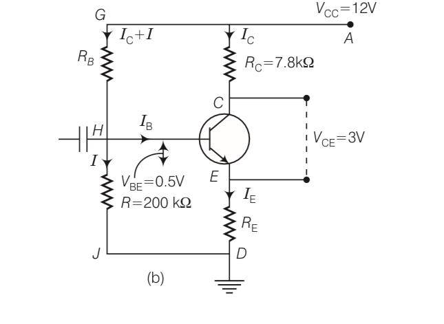
|
| 10. In the circuit diagram find the value of Rc
|
| Explanation- IE=IC+IB and Ic= IcRc+VCE+IERE=VCC RIB+VBE+IERE=Vcc IE=Ic= 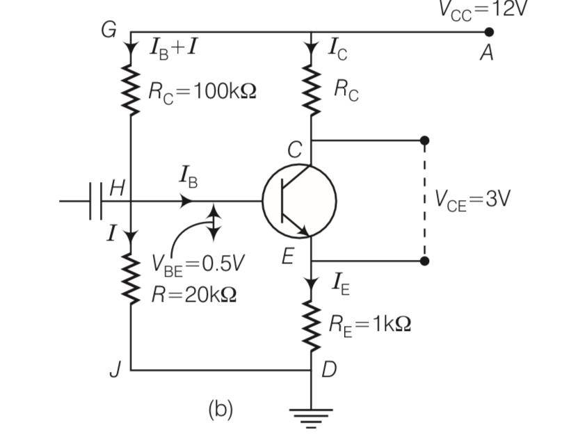
From above equation (R+ E)IB=VCC-VBE IB= ( )= ( )=1.56 Rc=1.56-1=0.56kohm |
Semiconductor Electronics Short Answer Type Questions
| 1. Why are elemental dopants for Silicon or Germanium usually chosen from group XIII or group XV? |
| Explanation-The size of the dopant atom should be such that their presence in the pure semiconductor does not distort the semiconductor but easily contribute the charge carriers on forming covalent bonds with Si or Ge atoms, which are provided by group XIII or group XV elements. |
| 2. Sn, C and Si, Ge are all group XIV elements. Yet, Sn is a conductor, C is an insulator while Si and Ge are semiconductors. Why? |
| Explanation- A material is a conductor if in its energy band diagram, there is no energy gap between conduction band and valence band. For insulator, the energy gap is large and for semiconductor the energy gap is moderate. The energy gap for Sn is 0 eV, for C is 5.4 eV, for Si is 1.1 eV and for Ge is 0.7 eV, related to their atomic size. Therefore Sn is a conductor, C is an insulator and Ge and Si are semiconductors. |
| 3. Can the potential barrier across a p-n junction be measured by simply connecting a voltmeter across the junction? |
| Explanation- We cannot measure the potential barrier across a p-n junction by a voltmeter because the resistance of voltmeter is very high as compared to the junction resistance. |
| 4. Draw the output waveform across the resistor in the given figure. 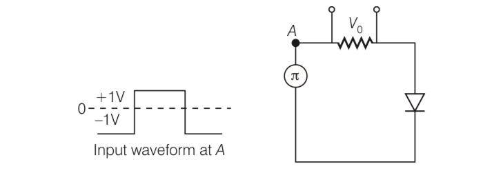
|
| Explanation- diode only works in forward biased. So output waveform is 
|
| 5. The amplifiers X, Y and Z are connected in series. If the voltage gains of X, Y and Z are 10,20 and 30, respectively and the input signal is 1 mV peak value, then what is the output signal voltage (peak value). |
| Explanation- as we know total voltage amplification = Avx= 10,Avy = 20,Avz = 30 vi = 1mV= 10-3V So according to formula = (Avx )(Avy )(Avz) vo = (Avx )(Avy )(Avz) vi = 10-3 =6V So in first case output cannot be greater than than 6V but in 2nd case it will work |
| 6. In a CE transistor amplifier, there is a current and voltage gain associated with the circuit. In other words there is a power gain. Considering power a measure of energy, does the circuit violate conservation of energy? |
| Explanation- In CE transistor amplifier, the power gain is very high. In this circuit, the extra power required for amplified output is obtained from DC source. Thus, the circuit used does not violet the law of conservation. |
| 7. (i) Name the type of a diode whose characteristics are shown in figure (a) and (b).
|
| Explanation- (i) The characteristic curve (a) is of Zener diode and curve (b) is of solar cell. (ii) The point P in fig. (a) represents Zener break down voltage. (iii) In fig. (b), the point Q represents zero voltage and negative current. It means light falling on solar cell with atleast minimum threshold frequency gives the current in opposite direction to that due to a battery connected to solar cell. But for the point Q, the battery is short circuited. Hence represents the short circuit current. In fig. (b), the point P represents some positive voltage on solar cell with zero current Through solar cell.It means, there is a battery connected to a solar cell which gives rise to the equal and Opposite current to that in solar cell by virtue of light falling on it. As current is zero for point P, hence we say P represents open circuit voltage. |
| 8. Three photo diodes D1, D2and D3 are made of semiconductors having band gaps of 2.5 eV, 2 eV and 3 eV, respectively. Which ones will be able to detect light of wavelength 6000 Å ? |
| Explanation- E=hc/ = = 2.06eV The incident radiation which is detected by the photodiode having energy should be greater Than the band-gap. So ,it is only valid for diode D2.Then,diode D2 will detect this radiation. |
| 9. If the resistance R1is increased (see figure), how will the readings of the ammeter and voltmeter change? 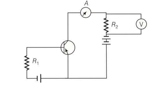
|
| Explanation- as base current IB = As Ri is increased IB is decreased. 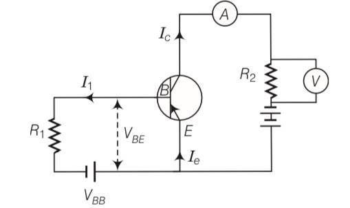
And collector current is Ic = IB as IB decreased Ic also decreased and the rading of voltmeter and ammeter also decreased. |
| 10. Two car garages have a common gate which needs to open automatically when a car enters either of the garages or cars enter both. Draw a circuit that resembles this situation using diodes for this situation. 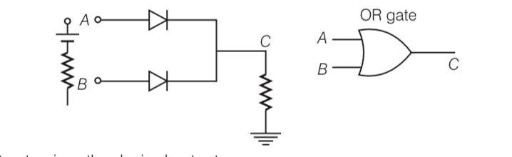
|
|||||||||||||||
| Explanation- OR gate gives the desired output.
|
| 11. How would you set up a circuit to obtain NOT gate using a transistor? |
||||||
| Explanation- The NOT gate is a device which has only one input and one output i.e., A’=Y means Y equals NOT A. 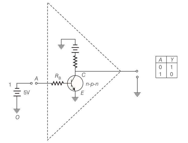
This gate cannot be realised by using diodes. However it can be realised by making use of a transistor. This can be seen in the figure given below.
Here, the base B of the transistor is connected to the input A through a resistance Rb and the emitter E is earthed. The collector is connected to 5 V battery. The output Y is the voltage at C w.r.t. earth. The resistor Rb and Rc are so chosen that if emitter-base junction is unbiased, the transistor is in cut off mode and if emitter-base junction is forward biased by 5V, the transistor is in saturation state. |
| 12. Explain why elemental semiconductor cannot be used to make visible LEDs. |
| Explanation- In elemental semiconductor, the band gap is such that the emission are in infrared region and not in visible region. |
| 13. Write the truth table for the circuit shown in figure given below. Name the gate that the circuit resembles. 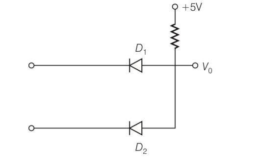
|
|||||||||||||||
| Explanation- this is AND gate so truth table for this will be
|
| 14. A Zener of power rating 1 W is to be used as a voltage regulator. If Zener has a breakdown of 5 V and it has to regulate voltage which fluctuated between 3 V and 7 V, what should be the value of Rs for safe operation (see figure)? 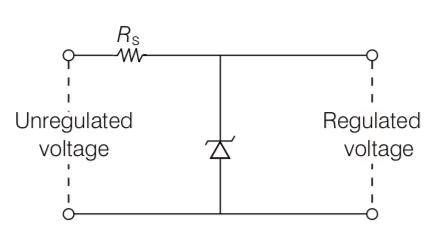
|
Semiconductor Electronics Multiple Choice Questions
| 1. The conductivity of a semiconductor increases with increase in temperature, because |
| Answer-(d) Explanation- when we increase temperature conductivity increases because number density is increasing after increasing temperature which decreases the relaxation time |
| 2. In figure given below V0 is the potential barrier across a pn junction when no battery is connected across the junction 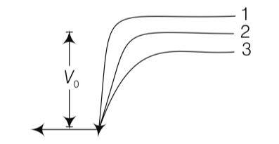
(a) 1 and 3 corresponds to forward bias of junction (b) 3 corresponds to forward bias of junction and 1 corresponds to reverse bias of the junction (c) 1 corresponds to forward bias and 3 corresponds to reverse bias of the junction (d) 3 and 1 both corresponds to reverse bias of the junction |
| Explanation - When p-n junction is forward biased, it opposes the potential barrier junction, when p-n junction is reverse biased, it supports the potential barrier junction, resulting increase in potential barrier across the junction. |
| 3. In figure given on next page, assuming the diodes to be ideal 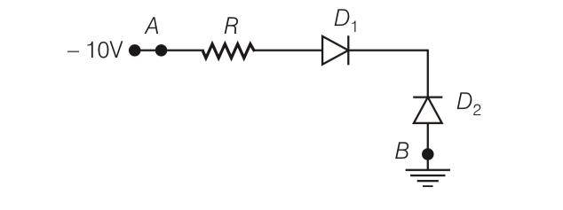
|
| Answer-b Explanation- from the figure we can say that that diode D1 is reverse biased and diode D2 is forward biased so current will flow from B to A. |
| 4. A 220 V AC supply is connected between points A and B (figure). What will be the potential difference V across the capacitor? 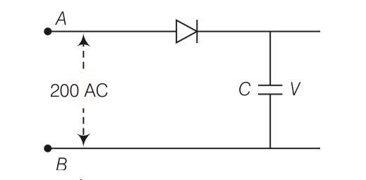
|
| Answer- d Explanation- as we know that Ev = Eo/ so E0= Ev so net voltage is 220 V |
| 5. Hole is |
| Answer-b Explanation -when a neutral entity is there it contains both equal number of elctron and holes. Also when electron emit from neutral entity then it leave behind a vacancy that is hole. |
| 6. The output of the given circuit in figure is given below. 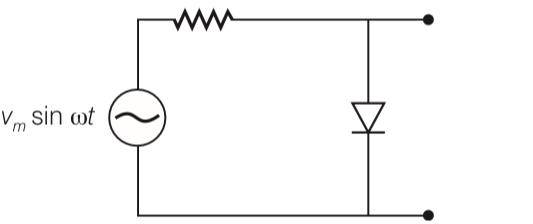
(a) would be zero at all times
(b) would be like a half wave rectifier with positive cycles in output |
| Answer- c Explanation- due to forward biasing the diffusion current in the circuit is very high and resistance in the circuit is very low. Thus voltage across pn junction is very low but in case of reverse biasing diffusion current very small so resistance becomes very high . and that end making high voltage across pn junction. |
| 7. In the circuit shown in figure given below, if the diode forward voltage between A and B is
|
| Answer-b Explanation- r1=5kohm and r2= 5kohm and both are in series Then V-0.3 = [(r1+r2)103] [0.2 10-3] V-0.3= 2 V= 2.3V |
| 8. Truth table for the given circuit is 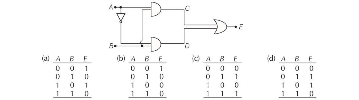
|
||||||||||||||||||||||||||||||
| Answer- c Explanation- C=A.B and D=A’B E= C+D = (A.B)+(A’.B)
|
| 9. When an electric field is applied across a semiconductor |
| Answer- (a,c) Explanation- when we apply temperature across semiconductor then electron will starts from lower energy to high energy level that is from valence band to conduction band. When electron goes from lower to higher then holes that is left behind they goes to lower energy levels. |
| 10. Consider an n-p-n transistor with its base-emitter junction forward biased and collector base junction reverse biased. Which of the following statements are true?
|
| Answer- a,c Explanation- Here emitter-base junction is forward biased i.e., the positive pole of emitter base battery is connected to base and its negative pole to emitter. Also, the collector base junction is reverse biased, i.e., the positive pole of the collector base battery is connected to collector and negative pole to base. Thus, electron move from emmiter to base and cross over from emitter to collector. |
| 11. In a n-p-n transistor circuit, the collector current is 10 mA. If 95 per cent of the electrons emitted reach the collector, which of the following statements are true? |
| Answer- b,c Explanation- IC= 10mA Ic= 95/100 Ie Ie= = 10.53mA Ib=Ie-IC= 10.53-10= .53mA |
| 12. In the depletion region of a diode |
| Answer- a,b,d Explanation- The space-charge regions on both the sides of p-n junction which has immobile ions and entirely lacking of any charge carriers will form a region called depletion region of a diode. The number of ionized acceptors on the p -side equals the number of ionized donors on the n-side. |
| 13. What happens during regulation action of a Zener diode? |
| Answer-b,d Explanation- During regulation action of a Zener diode, the current through the Rs changes and resistance offered by the Zener changes. The current through the Zener changes but the voltage across the Zener remains constant. |
| 14. To reduce the ripples in rectifier circuit with capacitor filter |
| Answer- a,c,d Explanation-ripple factor is inversely proportional to RL, C and frequency. so to reduce ripple factor all these should be increase. |
| 15. The breakdown in a reverse biased p-n junction is more likely to occur due to |
| Answer-(a,d) Explanation- In reverse biasing, the minority charge carriers will be accelerated due to reverse biasing, which on striking with atoms cause ionization resulting secondary electrons and thus more number of charge carriers. When doping concentration is large, there will be large number of ions in the depletion region, which will give rise to a strong electric field. |
Physics NCERT Exemplar Solutions Class 12th Chapter Fourteen Exam