

Semiconductor Electronics: Materials, Devices and
Get insights from 121 questions on Semiconductor Electronics: Materials, Devices and, answered by students, alumni, and experts. You may also ask and answer any question you like about Semiconductor Electronics: Materials, Devices and
Follow Ask QuestionQuestions
Discussions
Active Users
Followers
New question posted
10 months ago
New answer posted
10 months ago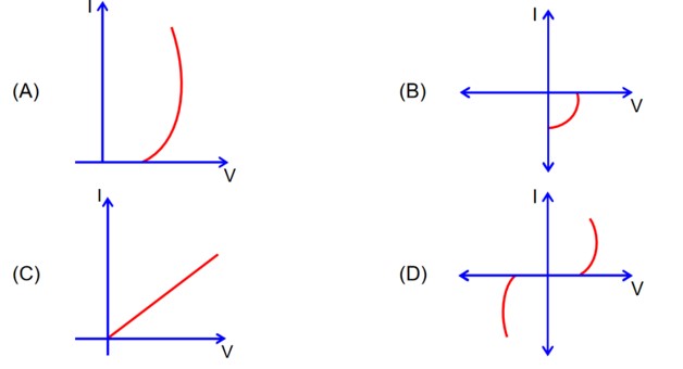
Contributor-Level 10
V-l characteristics graph is plotted in 4th quadrant for solar cell.
New answer posted
10 months ago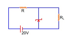
Contributor-Level 10
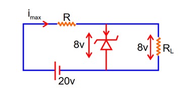
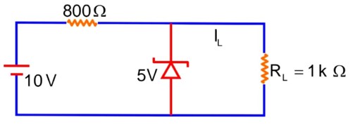
20 – imax R – 8 = 0
imax R = 12

At maxm zener current –
imaxR = 12v
25 * 10-3 R = 12
New answer posted
10 months ago
New answer posted
10 months ago
Contributor-Level 10
20 – imax R – 8 = 0
imax R = 12
At minimum zener current
At maxm zener current –
imaxR = 12v
25 * 103 R = 12
New answer posted
10 months agoContributor-Level 10
Ib = 10 µA
IC = 1.5 mA
RL = 50 kW or (Rc)
Base – emitter voltage = 10 mv
=
Av = 750
Taking an Exam? Selecting a College?
Get authentic answers from experts, students and alumni that you won't find anywhere else
Sign Up on ShikshaOn Shiksha, get access to
- 66k Colleges
- 1.2k Exams
- 699k Reviews
- 1850k Answers