

Semiconductor Electronics: Materials, Devices and
Get insights from 121 questions on Semiconductor Electronics: Materials, Devices and, answered by students, alumni, and experts. You may also ask and answer any question you like about Semiconductor Electronics: Materials, Devices and
Follow Ask QuestionQuestions
Discussions
Active Users
Followers
New answer posted
10 months ago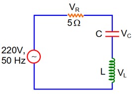
Contributor-Level 10
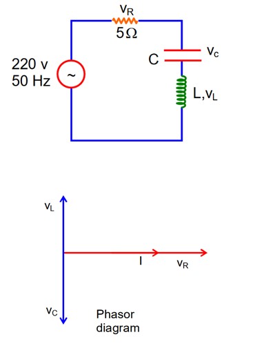
Given
VL = VC = 2VR, f = 50Hz
since, VL = VC.
then
VR = VNet = 220V
I =
= I xL = 440
xL = 10
WL = 10
2πfL = 10
New answer posted
a year agoBeginner-Level 5
A p-type semiconductor is electrically neutral despite having more holes, because the number of positively charged holes is exactly balanced/equal by the number of negatively charged acceptor ions introduced during doping. so practically untill any volatage is applied the semiconductor remains chargeless in other words doesn't produce any current even after doping.
As per the NCERT Textbooks information"Although the number of holes is more than the number of electrons in a p-type semiconductor, the material as a whole is electrically neutral because the charge of holes is balanced by the negatively charged acceptor ions.”
New answer posted
a year agoBeginner-Level 5
As per NCERT Textbboks"If forward current is too large, it can produce large heating and damage the junction. So, a resistor is used in series with the diode to limit the current in the circuit.”
It means when a semiconductor diode is connected to a source under high current it causes excess heat due to more electrical energy. This excess heat is responsible to damage the junction in semiconductor diode permanently. Student can check out NCERT Solutions for Semicondutor Electronics of class 12 physics.
New answer posted
a year ago
Contributor-Level 10
14.15 A acts as two inputs of the NOR gate and Y is the output. As shown in the following figure. Hence the output of the circuit is =

The truth table for the same is given as:
A | Y = ( ) |
0 | 1 |
1 | 0 |
This is the truth table of a NOT gate. Hence, this circuit functions as a NOT gate.
A and B are the inputs and Y is the output of the given circuit. By using the result obtained in solution (a), we can infer that the outputs of the first two NOR gates are and , as shown in the following figure

Above is given the inputs for the last NOR gate.
Hence, the output for the circuit can be written as:
Y = = = A.B
The truth table for the same can b
New answer posted
a year ago
Contributor-Level 10
14.14 A and B are the inputs of the given circuit. The output of the first NOR gate is + . It can be observed from the following figure that the inputs of the second NOR gate become the output of the first one.

Hence, the output of the combination is given as:
Y = = + = = = + =
The truth table for this operation is given as:
This is the truth table of an or gate. Hence, this circuit functions as an or gate.
A | B | Y ( = A + B) |
0 | 0 | 0 |
0 | 1 | 1 |
1 | 0 | 1 |
1 | 1 | 1 |
This is the truth table of an OR gate. Hence, this circuit functions as an OR gate.
New answer posted
a year ago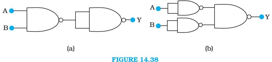
Contributor-Level 10
14.13 The output of the left NAND gate will be , as shown in the following figure:

Hence, the output of the combination of two NAND gates is given as:
Y = ( ).( ) = + = AB
Hence the circuit functions as an AND gate.
is the output of the upper left of the NAND gate and is the output of the lower half of the NAND gate, as shown in the following figure.

Hence, the output of the combination of the NAND gates will be given as:
Y = . = + = A + B
Hence, this circuit functions as an OR gate.
New answer posted
a year ago
Contributor-Level 10
14.12 A acts as the two inputs of the NAND gate and Y is the output, as shown in the following figure.

Hence, the output can be written as:
Y = = + = ……………(i)
The truth table for equation (i) can be drawn as:
A | Y = ( ) |
0 | 1 |
1 | 0 |
This circuit functions as a NOT gate. The symbol for this logic circuit is as shown below:

New answer posted
a year ago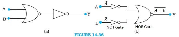
Contributor-Level 10
14.11 A and B are the inputs and Y is the output of the given circuit. The left half of the given figure acts as the NOR gate, while the right half acts as the NOT gate

Hence the output of the NOR gate is
This will be input for the NOT gate. Its output will be = A + B
So Y = A + B
Hence, this circuit functions as an OR gate.
A and B are the inputs and Y is the output of the given circuit. It can be observed from the following figure that the inputs of the right half NOR gate are the outputs of the two NOT gates.

Hence, the output of the given circuit can be written as:
Y = = = A + BHence this circuit functions as an AND gate.
New answer posted
a year agoContributor-Level 10
14.10 In a p-n junction diode, the expression for current is given as:
Where, = Reverse saturation current = 5 A
T = Absolute temperature = 300 K
= Boltzmann constant = 8.6 eV/K = 8.6 J/K = 1.376
V = voltage across the diode
e = charge of an electron = 1.6 C
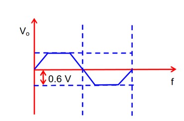
Forward voltage, V = 0.6V
Current, =
= 0.02315 A
For forward voltage, V = 0.7V, we can write
Current, =
= 1.117 A
Hence increase in the current, ΔI = I'-I = 1.117 – 0.02315 = 1.0934 A
Dynamic resistance = =
If the reverse bias voltage is changed from 1 V to 2 V, the current will remain same as will be equal in both cases. Therefore
Taking an Exam? Selecting a College?
Get authentic answers from experts, students and alumni that you won't find anywhere else
Sign Up on ShikshaOn Shiksha, get access to
- 66k Colleges
- 1.2k Exams
- 699k Reviews
- 1850k Answers