

Semiconductor Electronics: Materials, Devices and
Get insights from 121 questions on Semiconductor Electronics: Materials, Devices and, answered by students, alumni, and experts. You may also ask and answer any question you like about Semiconductor Electronics: Materials, Devices and
Follow Ask QuestionQuestions
Discussions
Active Users
Followers
New answer posted
9 months ago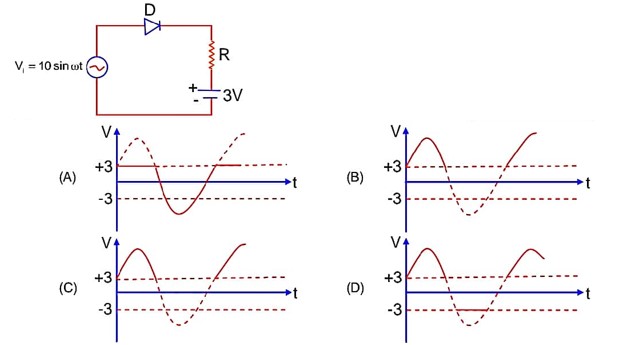
Contributor-Level 10
Diode, in forward biased condition only, will allow current to flow through it.
Pot. different across resistor is
But in reverse biased condition of diode,
(across diode)
New answer posted
9 months ago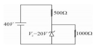
Contributor-Level 10
Potential difference across R?
(R? / (R? +R? ) * V is greater than zenor voltage
⇒ i? = V_z/R? = 20/1000 A = 20 mA
Current through R? , i? = (40-V_z)/R? = 20/500 = 40 mA
Current through zener diode = i? - i? = 20 mA
New answer posted
9 months ago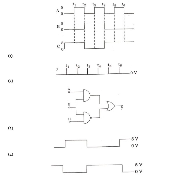
Contributor-Level 10
Y = A·B + B·C
(i) o to t? A = 0, B = 0, C = 1
(ii) Y = 0.0 + 0.1 = 0 + 1 = 1
(ii) t? to t? A = 1, B = 0, C = 1 Y = 1.0 + 0.1 = 0 + 1 = 1
(iii) t? to t? A = 0, B = 1, C = 0 Y = 0.1 + 0.1 = 0 + 1 = 1
New answer posted
9 months agoContributor-Level 10
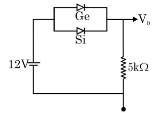
A reverse-biased Zener diode is used as a voltage regulator.
The potential barrier for Germanium (Ge) is approximately 0.3 V.
The potential barrier for Silicon (Si) is approximately 0.7 V.
New answer posted
9 months agoContributor-Level 10
In n-type semiconductor majority charge carriers are e- and P type semiconductor majority charge carriers are holes.
neA
Taking an Exam? Selecting a College?
Get authentic answers from experts, students and alumni that you won't find anywhere else
Sign Up on ShikshaOn Shiksha, get access to
- 66k Colleges
- 1.2k Exams
- 699k Reviews
- 1850k Answers