
Semiconductor Electronics: Materials, Devices and
Get insights from 121 questions on Semiconductor Electronics: Materials, Devices and, answered by students, alumni, and experts. You may also ask and answer any question you like about Semiconductor Electronics: Materials, Devices and
- 121
Questions
- 0
Discussions
- 0
Active Users
- 0
Followers
Have a question about Semiconductor Electronics: Materials, Devices and? Ask our experts
Keep it short & simple. Type complete word. Avoid abusive language.
Two Zener diodes (A and B) having breakdown voltages of 6 V and 4 V respectively, are connected as shown in the circuit below. The output voltage V? variation with input voltage linearly increasing with time, is given by: (V_input = 0 V at t = 0) (figures are qualitative)
<!--[endif]-->
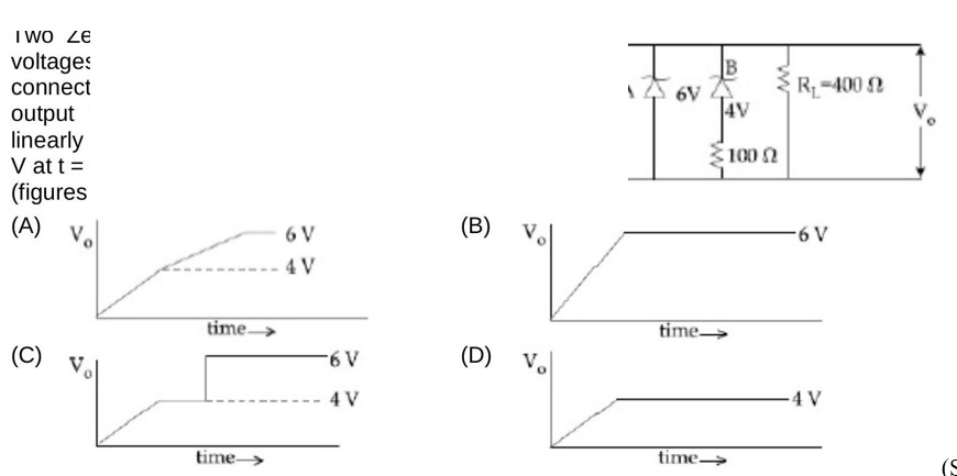
Two Zener diodes (A and B) having breakdown voltages of 6 V and 4 V respectively, are connected as shown in the circuit below. The output voltage V? variation with input voltage linearly increasing with time, is given by: (V_input = 0 V at t = 0) (figures are qualitative)
<!--[endif]-->
Till input voltage reaches 4 V. No zener is in breakdown region. So V? = V? then now hen V? changes between 4 V to 6 V one zener with 4 V will breakdown are P.D. across this zener will become constant and remaining potential will drop acro resistance in series with 4 V zener.
Now current in circuit i
 Upvote

Which of the following given a reversible operation?

Which of the following given a reversible operation?
A logic GATE is reversible if we can recover input data fro the output eg. NOT gate.
Upvote The following logic gate is equivalent to:
<!-- [if !supportLineBreakNewLine]-->
<!--[endif]-->
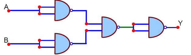
The following logic gate is equivalent to:
<!-- [if !supportLineBreakNewLine]-->
<!--[endif]-->
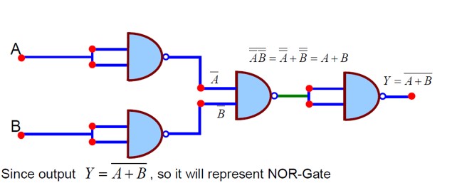
In a semiconductor, the number density of intrinsic charge carriers at 27°C is 1.5 × 10¹? / m³. If the semiconductor is doped with impurity atom, the hole density increases to 4.5×10²² / m³. The electron density in the doped semiconductor is __________ x 10? / m³.
In a semiconductor, the number density of intrinsic charge carriers at 27°C is 1.5 × 10¹? / m³. If the semiconductor is doped with impurity atom, the hole density increases to 4.5×10²² / m³. The electron density in the doped semiconductor is __________ x 10? / m³.
ni² = ne × nh
(1.5×10¹? )² = ne × (4.5×10²²)
ne = (2.25 × 10³²)/ (4.5 × 10²²) = 0.5 × 10¹? = 5 × 10? / m³
Upvote A transistor is connected in common emitter circuit configuration, then collector supply voltage is 10 V and the voltage drop across a resistor of 1000Ω in the collector is 0.6 V. If the current gain factor (β) is 24, then the base current is _______ µA. (Round off to the Nearest Integer)
A transistor is connected in common emitter circuit configuration, then collector supply voltage is 10 V and the voltage drop across a resistor of 1000Ω in the collector is 0.6 V. If the current gain factor (β) is 24, then the base current is _______ µA. (Round off to the Nearest Integer)
As we know, β = Ic/Ib = 24 (Given)
R = 1000Ω, ΔV = 0.6V, Ic = ΔV/R = 0.6/1000 = 6×10? A
So, Ib = Ic/β = (6×10? )/24 = 25×10? A
or Ib = 25µA
Upvote The zener diode has a Vz = 30V. The current passing through the diode for the following circuit is…………mA.
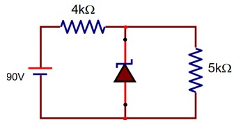
The zener diode has a Vz = 30V. The current passing through the diode for the following circuit is…………mA.
Draw the output signal Y in the given combination of gates.
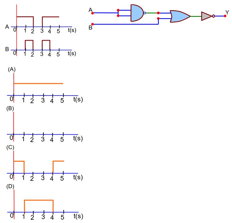
Draw the output signal Y in the given combination of gates.
The circuit contains two diodes each with a forward resistance of 50 and with infinite reverse resistance. If the battery voltage is 6 V, the current through the 120 resistance is---------mA.

The circuit contains two diodes each with a forward resistance of 50 and with infinite reverse resistance. If the battery voltage is 6 V, the current through the 120 resistance is---------mA.
D1 is forward biased & D2 is reverse biased.
Upvote Given below are two statements:
Statement I : PN junction diodes can be used to function as transistor simply by connecting two diodes, back to back, which acts as the base terminal.
Statement II : In the study of transistor, the amplification factor b indicates ratio of the collector current to the base current.
In the light of the above statements, choose the correct answer from the options given below.
Given below are two statements:
Statement I : PN junction diodes can be used to function as transistor simply by connecting two diodes, back to back, which acts as the base terminal.
Statement II : In the study of transistor, the amplification factor b indicates ratio of the collector current to the base current.
In the light of the above statements, choose the correct answer from the options given below.
A tristor is formed by doping a semi conductor water from one side by N-type dopant (high concentration while comparatively lower concentration on other side thus forming NPN tristor & vice-versa.
So, statement (I) is false & statement (II) is true.
Upvote