
Semiconductor Electronics: Materials, Devices and
Get insights from 121 questions on Semiconductor Electronics: Materials, Devices and, answered by students, alumni, and experts. You may also ask and answer any question you like about Semiconductor Electronics: Materials, Devices and
- 121
Questions
- 0
Discussions
- 0
Active Users
- 0
Followers
Have a question about Semiconductor Electronics: Materials, Devices and? Ask our experts
Keep it short & simple. Type complete word. Avoid abusive language.
Zener breakdown occurs in a P- n junction having P and n both:
Zener breakdown occurs in a P- n junction having P and n both:
Zener break down occurs in p-n junction having p and n both : Heavily doped and have narrow depletion layer.
 Upvote

A 5 V battery is connected across the points X and Y. Assume D1 and D2 to the normal silicon diodes. Find the current supplies by the battery if the +ve terminal of the battery is connected to point X.
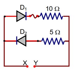
A 5 V battery is connected across the points X and Y. Assume D1 and D2 to the normal silicon diodes. Find the current supplies by the battery if the +ve terminal of the battery is connected to point X.
D1 is in forward bias and D2 is in reverse bias.
Current, I
Upvote <p><strong>Match List I with List II.</strong></p>
<p><strong>List I List II</strong></p>
<p><strong>(a)</strong> Rectifier <strong> (i) </strong>Used either for stepping up or stepping down the a.c. voltage</p>
<p><strong>(b)</strong> Stabilizer <strong> (ii)</strong> Used to convert a.c. voltage into d.c. voltage</p>
<p><strong>(c) </strong>Transformer <strong> (iii)</strong> Used to remove any ripple in the rectified output voltage</p>
<p><strong>(d) </strong>Filter <strong> (iv) </strong>Used for constant output voltage even when the input voltage or<strong> </strong>load current chage.</p>
<p><strong>Choose the correct answer from the options given below</strong></p>
For extrinsic semiconductors; when doping level is increased
For extrinsic semiconductors; when doping level is increased
Fermi level of p-type semiconductors will go downward
Upvote 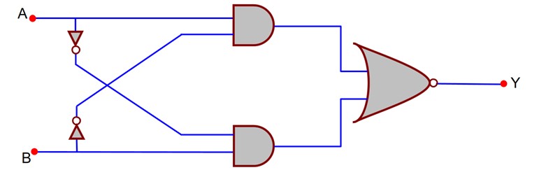
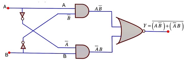
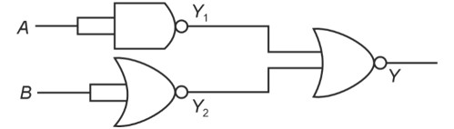
The output of the given logic gate is similar to the output of an/a
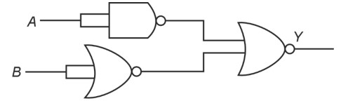
The output of the given logic gate is similar to the output of an/a
In an ideal transformer, the turns ratio is . The ratio is equal to (the symbols carry their usual meaning) :
In an ideal transformer, the turns ratio is . The ratio is equal to (the symbols carry their usual meaning) :
According to transformer ratio,
Upvote In the circuit shown below, maximum zener diode current will be _________mA.
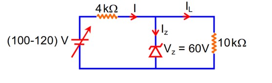
In the circuit shown below, maximum zener diode current will be _________mA.
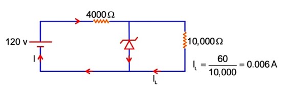
Thus l2 = l - LL
= 0.015 – 0.006
= 0.009 = 9mA
 Upvote
In a given circuit diagram, a 5 V zener diode along with a series resistance is connected across a 50 V power supply. The minimum value of the resistance required, if the maximum zener current is 90 mA be________ <!-- [if gte mso 9]><xml>

In a given circuit diagram, a 5 V zener diode along with a series resistance is connected across a 50 V power supply. The minimum value of the resistance required, if the maximum zener current is 90 mA be________ <!-- [if gte mso 9]><xml>
For 90 mA in zener diode, current in R should be greater than 90 mA.
Upvote Consider a situation in which reverse biased current of a particular P – N junction increase when it is exposed to a light of wavelength <!-- [if gte mso 9]><xml>
Consider a situation in which reverse biased current of a particular P – N junction increase when it is exposed to a light of wavelength <!-- [if gte mso 9]><xml>