
Semiconductor Electronics: Materials, Devices and
Get insights from 121 questions on Semiconductor Electronics: Materials, Devices and, answered by students, alumni, and experts. You may also ask and answer any question you like about Semiconductor Electronics: Materials, Devices and
- 121
Questions
- 0
Discussions
- 0
Active Users
- 0
Followers
Have a question about Semiconductor Electronics: Materials, Devices and? Ask our experts
Keep it short & simple. Type complete word. Avoid abusive language.
A full wave rectifier circuit consists of two p-n junction diodes, a centre-tapped transformer, capacitor and a load resistance. Which of these components remove the ac ripple from the rectified output
<!-- [if !supportLineBreakNewLine]-->
<!--[endif]-->
A full wave rectifier circuit consists of two p-n junction diodes, a centre-tapped transformer, capacitor and a load resistance. Which of these components remove the ac ripple from the rectified output
<!-- [if !supportLineBreakNewLine]-->
<!--[endif]-->
Time period of satellite
 Upvote

The typical output characteristics curve for a transistor working in the common-emitter configuration is shown in the figure.
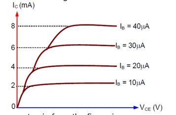
The estimated current gain from the figure is.
The typical output characteristics curve for a transistor working in the common-emitter configuration is shown in the figure.
The estimated current gain from the figure is.
β = I? /I? = (2 × 10? ³)/ (10 × 10? ) = 200
Upvote The correct relation between α (ratio of collector current to emitter current) and β (ratio of collector current to base current) of a transistor is :
<!-- [if !supportLineBreakNewLine]-->
<!--[endif]-->
The correct relation between α (ratio of collector current to emitter current) and β (ratio of collector current to base current) of a transistor is :
<!-- [if !supportLineBreakNewLine]-->
<!--[endif]-->
I? = I? + I? ⇒ I? /I? = 1 + I? /I? ⇒ 1/α = 1 + 1/β = (β+1)/β ⇒ α = β/ (1+β)
⇒ 1/β = 1/α - 1 = (1-α)/α ⇒ β = α/ (1-α)
Upvote The output of the given combination gates represents:
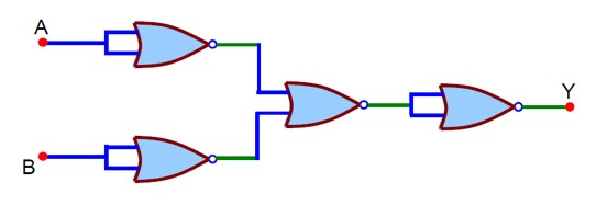
The output of the given combination gates represents:
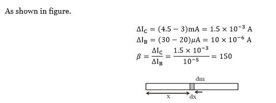
Kindly consider the following figure
Upvote The out put characteristics of a transistor is shown in the figure. When VCE is 10 V and Ic = 4.0 mA, then value of βac is
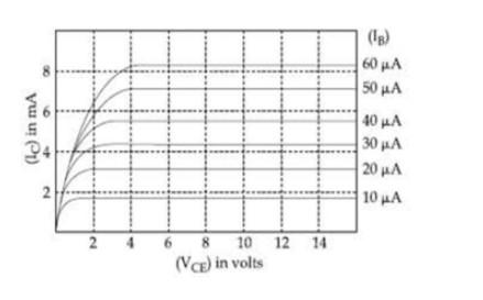
The out put characteristics of a transistor is shown in the figure. When VCE is 10 V and Ic = 4.0 mA, then value of βac is

Which of the following will NOT be observed when a multimeter (operating in resistance measuring mode) probes connected across a component, are just reversed?
Which of the following will NOT be observed when a multimeter (operating in resistance measuring mode) probes connected across a component, are just reversed?
Multimeter will show deflection when current will flow to charge the capacitor.
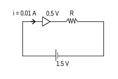
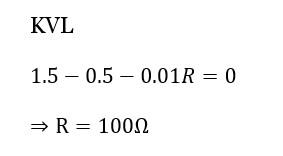
Upvote When a diode is forward biased, it has a voltage drop of 0.5 V. The safe limit of current through the diode is 10 mA. If a battery of emf 1.5 V is used in the circuit, the value of minimum resistance to be connected in series with the diode so that the current does not exceed the safe limit is
<!-- [if !supportLineBreakNewLine]-->
<!--[endif]-->
When a diode is forward biased, it has a voltage drop of 0.5 V. The safe limit of current through the diode is 10 mA. If a battery of emf 1.5 V is used in the circuit, the value of minimum resistance to be connected in series with the diode so that the current does not exceed the safe limit is
<!-- [if !supportLineBreakNewLine]-->
<!--[endif]-->
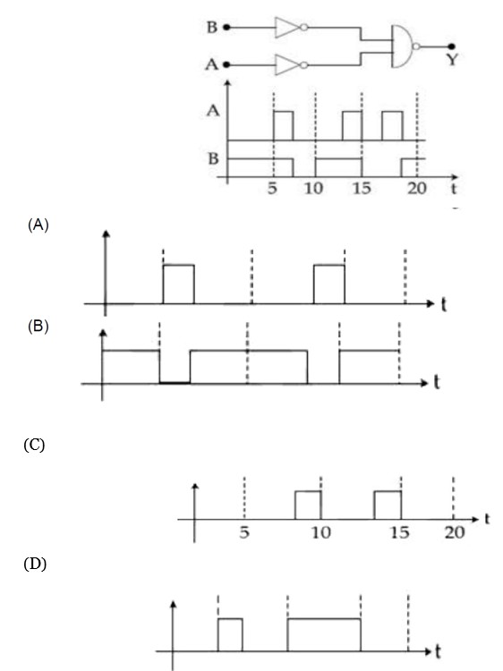
Identify the correct output signal Y in the given combination of gates (as shown) for the given inputs A and B.
<!-- [if !supportLineBreakNewLine]-->
<!--[endif]-->
Identify the correct output signal Y in the given combination of gates (as shown) for the given inputs A and B.
<!-- [if !supportLineBreakNewLine]-->
<!--[endif]-->
Kindly consider the following figure
Upvote