

Semiconductor Electronics: Materials, Devices and
Get insights from 121 questions on Semiconductor Electronics: Materials, Devices and, answered by students, alumni, and experts. You may also ask and answer any question you like about Semiconductor Electronics: Materials, Devices and
Follow Ask QuestionQuestions
Discussions
Active Users
Followers
New answer posted
10 months agoContributor-Level 10
Active region of the CE transistor is linear region and is best suited for its use as an amplifier.
New answer posted
10 months agoContributor-Level 10
Pentavalent materials have more electrons and so electron density increase. But overall semiconductor is neutral
New answer posted
10 months agoContributor-Level 10
Very small change in minority charge carriers produces high value of reverse bias current.
New answer posted
10 months ago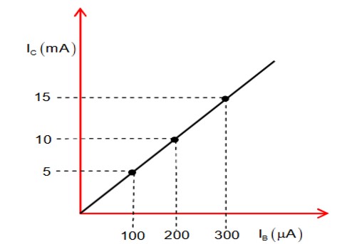
Contributor-Level 10
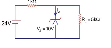
Voltage gain =
R0 ->Output Resistance
Ri ->Input Resistance
IC ->Collector current
IB ->Base current
Voltage gain =
New answer posted
10 months ago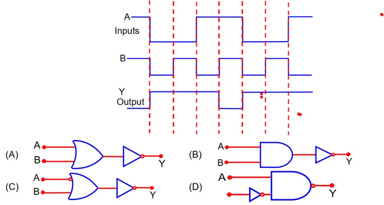
Contributor-Level 10
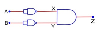
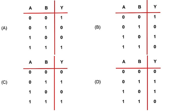
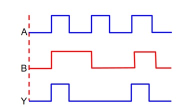
Truth table for Input & Output
A | B | y |
1 | 1 | 0 |
0 | 0 | 1 |
0 | 1 | 1 |
1 | 0 | 1 |
1 | 1 | 0 |
0 | 0 | 1 |
0 | 1 | 1 |
1 | 0 | 1 |
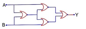
Now, Truth Table for option B.
A | B | y |
1 | 1 | 0 |
1 | 0 | 1 |
0 | 1 | 1 |
0 | 0 | 1 |
Taking an Exam? Selecting a College?
Get authentic answers from experts, students and alumni that you won't find anywhere else
Sign Up on ShikshaOn Shiksha, get access to
- 66k Colleges
- 1.2k Exams
- 699k Reviews
- 1850k Answers