
Semiconductor Electronics: Materials, Devices and
Get insights from 121 questions on Semiconductor Electronics: Materials, Devices and, answered by students, alumni, and experts. You may also ask and answer any question you like about Semiconductor Electronics: Materials, Devices and
- 121
Questions
- 0
Discussions
- 0
Active Users
- 0
Followers
Have a question about Semiconductor Electronics: Materials, Devices and? Ask our experts
Keep it short & simple. Type complete word. Avoid abusive language.
In the voltage regulator circuit shown below, the reverse breakdown voltage of zener diode is 3 V. Find the current through zener diode.
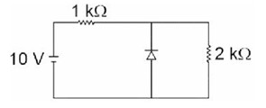
In the voltage regulator circuit shown below, the reverse breakdown voltage of zener diode is 3 V. Find the current through zener diode.
ibattery=
i2kW =
iz = (7 – 1.5) mA
= 5.5mA
 Upvote

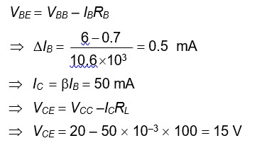
For the transistor circuit as shown. If b = 100, voltage drop between emitter and base is 0.7 V then value of VCE will be:-
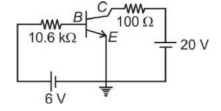
For the transistor circuit as shown. If b = 100, voltage drop between emitter and base is 0.7 V then value of VCE will be:-
Avalanche breakdown of p-n junction diode is due to
Avalanche breakdown of p-n junction diode is due to
In reverse biasing, due to collision of electrons and atom, avalanche breakdown occurs.
Upvote What is the current through an ideal P – N junction diode shown in figure below?
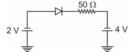
What is the current through an ideal P – N junction diode shown in figure below?
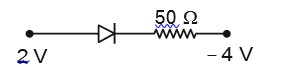
In a transistor if and . If varies between and , then the value of lies between
In a transistor if and . If varies between and , then the value of lies between
The relation between and is given as
Upvote Statement A: In intrinsic semiconductors, conductivity is mainly due to the breakage of covalent bonds.
Statement B: In extrinsic semiconductors, the conductivity is mainly due to the addition of impurities.
Statement A: In intrinsic semiconductors, conductivity is mainly due to the breakage of covalent bonds.
Statement B: In extrinsic semiconductors, the conductivity is mainly due to the addition of impurities.
In intrinsic semiconductors, conductivity is mainly due to breakage of covalent bonds in extrinsic semiconductors, the conductivity is due to the addition of impurities.
Upvote An AND gate can be prepared by repetitive use of
a) NOT gate (b) OR gate (c) NAND gate (d) NOR gate
An AND gate can be prepared by repetitive use of
a) NOT gate (b) OR gate (c) NAND gate (d) NOR gate
On repetitive use of NAND GATE or NOR gate, any logic GATE can be prepared.
Upvote In a transistor if and . If varies between and , then the value of lies between
In a transistor if and . If varies between and , then the value of lies between
The relation between and is given as
Upvote What is the current through an ideal P – N junction diode shown in figure below?
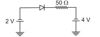
What is the current through an ideal P – N junction diode shown in figure below?