 / Preparation Physics Semiconductor Devices
P-N Junction is the fundamental concept of building various semiconductor devices like diodes, transistors, solar cells, etc. It is formed by diffusing trivalent and pentavalent impurities on each side of p-n junctions. When a p-type and n-type region is joined, a depletion layer is formed, which allows the flow of current in one direction and opposed in the opposite or reverse direction. This behaviour is essential for signal processing and rectification.
The behaviour of the p-n junction differs based on its connection. In forward bias, the junction conducts electricity and resists the current flow in reverse bias. Students can refer to this article for detailed knowledge of p-n junction definition, formation, working principle, types, etc.
Mastering the p-n junction topic is essential to understanding the Class 12 Physics Chapter 14 Semiconductor. This topic is essential for both CBSE board exam and competitive tests, such as JEE Main, NEET, etc. Further, it will lay the foundation for higher education in electrical engineering, electronics, and quantum physics.
Students can also refer the Class 12 Physics Chapter 14 Semiconduction NCERT solutions for intext and exercise problems. The subject experts at Shiksha have prepared the NCERT Class 12 Physics solution to guide students in their preparation for board exam. Furthermore, NCERT Solutions is the best guide for securing decent marks in the exam.
- P-N Junction Definition
- Types of P-n Junction
- Working Principal of P-N junction
- Formation of p-n Junction
- Circuit Symbol for a p-n Junction Diode
- Example of P-N Junction
P-N Junction Definition
The defination of p-n junction as per the NCERT is “A p-n junction is the basic building block of many semiconductor devices like diodes, transistors, etc”.
Explanation: P-N Junction is a semiconductor device that is used to make the base of electronic components such as diodes, transistors, etc.
Importance of P-N Junction
As mentioned in the definition, p-n junction is used to make the base of electronic components. Below is the importance.
Rectifier: P-N Junction can allow the flow of current in one direct (forward bias) and block the current in opposite direction (reverse bias). Due to this property, it is used for converting the AC (Alternate Current) to DC (Direct Current).
Switching: As mentioned above p-n junction can allow the flow of current in one direction, it can be used as a switch in semiconductors to control the flow of current and blocking in the other end.
Signal Processing: P-N Junction is also used in signal circuits to display the clip, rectify the signal, and or clamp.
Form Basis of Transistors: Multiple p-n junctions are used to build the bases of transistors such as BJT and MOSFETs.
Building Block for Integrated Circuits: Millions or billions of P-N junctions are used to build an integrated circuit (IC). Building Modern microprocessors, memory chips, and digital devices are possible because of p-n junction.
Other Applications:
- Solar Cells: P-N junctions are used to convert sunlight into electricity
- LED (Light Emitting Diodes) - When p-n junction is under forward bias, led produces light.
- Photodiodes: Photodiodes are P-N junctions under reverse bias that convert light into electrical current.
Types of P-n Junction
A p-n junctions are classified based on application, structure and operations. Below is the type of p-n junction.
- Unbiased P-N Junctions
- Forward biased
- Reversed biased
- Step-graded
- Linearly graded
- Heterojunction
- Schottky junction
Features of P-N Junctions
| Types of p-n junctions |
Features |
| Unbiased |
No external voltage |
| Forward biased |
p-side positive, n-side negative, current flow in the same direction |
| Reversed biased |
p-side negative, block current |
| Step-graded |
Sudden doping change |
| Linearly graded |
Slow doping change |
| Heterojunction |
Two different semiconductors with different band gaps |
| Schottky junction |
Metal semiconductor junction |
Working Principal of P-N junction
P-N junction working principle is based on the movement of charge carriers from n-type (electron rich) and p-type (hole-rich) semiconductor when brought together. This interaction forms a depletion region.
Working of P-N Junction:
Diffusion of Charge Carriers
- When p and n-type junction are joined, electrons from the n-type and holes from the p-type diffuse across the junction.
- The electrons and holes are recombined near the junction due to the diffusion process.
Formation of Depletion Region
- The diffusion leaves behind fixed ions – negative ions on the p-side and positive ions on the n-side.
- The immobile ions' charge forms a depletion region, which opposes further diffusion.
Built-in Potential (Barrier Potential)
- A potential barrier is built due to the electric field across the depletion region.
- Due to this barrier, the flow of charge carriers across the junction is opposed.
Behavior under external voltage:
Forward Bias
- In forward bias the positive side of voltage source is connected to positive terminal (anode) and negative terminal (cathode).
- The external voltage reduces the width of depletion region. This allows the electrons and holes to flow through the junction (p to n side).
Reverse Bias
- In reversed bias, the positive side of external voltage source is connected to negative side and negative to positive side.
- The voltage widens the Depletion region, due to which almost no current flows across the junction.
- Current flow is blocked in the reverse-bias junction.
Formation of p-n Junction
A
-n junction is not the interface between p -type and n - type semiconductor crystals pressed together. It is a single piece of semiconductor crystal having an excess of acceptor impurities into one side and of donor impurities into the other.
(b) Potential Barrier at the Junction: Formation of Depletion Region:
A p-n junction is shown in Fig. The p-type region has (positive) holes as majority charge-carriers, and an equal number of fixed negatively-charged acceptor ions. (The material as a whole is thus neutral). Similarly, the n -type region has (negative) electrons as majority charge-carriers, and an equal number of fixed positively-charged donor ions.
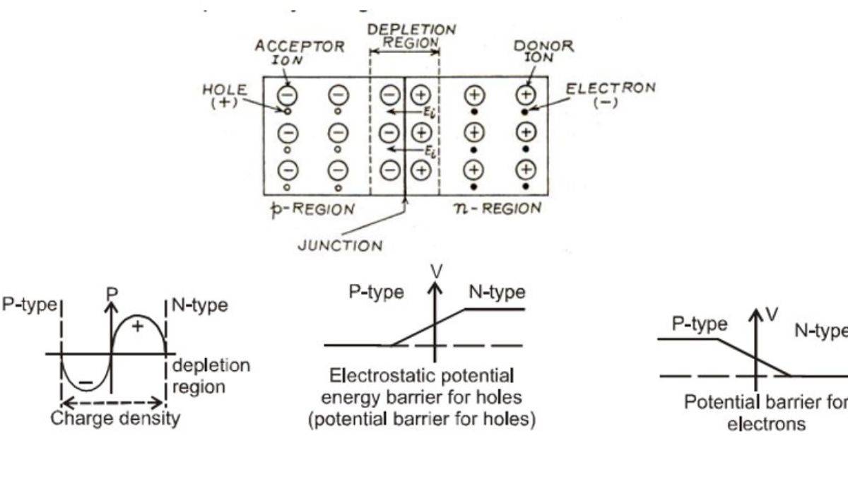
Electrostatic potential energy barrier for holes (potential barrier for holes)
The region on either of the junction which becomes depleted (free) of the mobile charge-carriers is called the 'depletion region'. The width of the depletion region is of the order of
. The potential difference developed across the depletion region is called the 'potential barrier'. It is about 0.3 volt for Ge, p-n junction and about 0.7 volt for silicon
junction. It, however, depends upon the dopant concentration in the semiconductor.
The magnitude of the barrier electric field for a silicon junction is
Diffusion & Drift Current : Due to concontration difference hole try to diffuse from p side to n side but due to depletion layer only those hole are able to diffuse from p to n side which have high kinetic energy. Similarly electron of high kinetic energy also diffuse from
to
so diffusion current flow from p to n side.
Due to thermal collision or increase in temperature some valence electron comes in conduction band. If this occurs in depletion region then hole move towards
side & electron move towards n side so a current produce from
to
side. It is called drift current, in steady state both diffusion & drift current are equal & opposite.
Circuit Symbol for a p-n Junction Diode
In electronic circuits, the semiconductor devices are represented by their symbols. The symbol for the basic device, the p -n junction diode, is shown
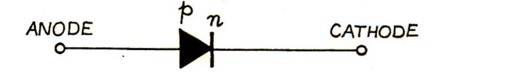
in Fig. The arrow-head represents the
-region and the bar represents the n -region of the diode.
The direction of the arrow is from p to n and indicates the direction of conventional current flow under forward bias. The p -side is called 'anode' and the n -side is called 'cathode'.
Example of P-N Junction
P-N junctions are the basic of building many semiconductor devices from simple diodes to complex transistors and optoelectronic devices. Here are the examples of P-N junctions and their key role.
Example of p-n junction
| Device | Role of P-N Junction |
| Solar Cell | Convert light to electricity |
| LED | Emission of light under forward bias |
| Photodiode | Detection of light under reverse bias |
| Diode | One-way current flow |
| Zener Diode | Voltage regulation |
| Tunnel Diode | Negative resistance |
| BJT | Amplification and switching |
| Varactor Diode | Variable capacitance |
Physics Semiconductor Devices Exam
Student Forum
Other Class 12th Physics Chapters
- Physics Alternating Current
- Physics Ray Optics and Optical Instruments
- Physics Electromagnetic Induction
- Physics Dual Nature of Radiation and Matter
- Physics Semiconductor Devices
- Physics Wave Optics
- Physics Current Electricity
- Physics Nuclei
- Physics Electrostatic Potential and Capacitance
- Physics Atoms
- Physics Moving Charges and Magnetism
- NCERT Class 12 Notes
- NCERT Class 12 Physics
- Physics Electric Charge and Field
- Physics Electromagnetic Waves
- Physics Magnetism and Matter