 / Preparation Physics Semiconductor Devices
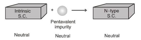
An extrinsic semiconductor is made by intentionally doping an intrinsic semiconductor with small amounts of impurities. The aim of doping an intrinsic semiconductor is to change its electrical conductivity. One can do this by creating N-type or P-type semiconductors. The conductivity of a semiconductor depends on its temperature, but at room temperature, its conductivity is very low. As such, no important electronic devices can be developed using these semiconductors. Hence, there is a necessity to improve their conductivity. This can be done by making use of impurities. When a small amount, say, a few parts per million (ppm), of a suitable impurity is added to the pure semiconductor, the conductivity of the semiconductor is increased manifold. Such materials are known as extrinsic semiconductors or impurity semiconductors.
The process of intentionally adding desirable impurity is called doping, and the impurity atoms that are added are called dopants. This type of material is also known as a doped semiconductor. Do remember that the dopant must not distort the original pure semiconductor lattice. The dopant only occupies a very few of the original semiconductor atom sites in the crystal. For this to happen, sizes of both dopant and semiconductor atoms should be nearly the same. There are two types of dopants that are used in doping tetravalent Si or Ge:
- Pentavalent (valency 5); Arsenic (As), Antimony (Sb), Phosphorous (P), etc.
- Trivalent (valency 3); Indium (In), Boron (B), Aluminium (AI), etc.
Si and Ge belong to the fourth group in the Periodic table, and, therefore, we should choose the dopant element from the nearby fifth or third group since the size of the dopant atom is nearly the same as that of Si or Ge. Interestingly, the pentavalent and trivalent dopants in Si or Ge give two entirely different types of semiconductors.
- What is Extrinsic Semiconductor?
- Types of Extrinsic Semiconductor
- N-Type Extrinsic semiconductor
- Some important facts about N-Type Semiconductor
- P-type semiconductor
- Some important facts about P-Type Semiconductor
- Electrical conductivity of extrinsic semiconductors
- Extrinsic Semiconductor Equations
- About the Reviewer
What is Extrinsic Semiconductor?
An extrinsic semiconductor is another type of semiconductor that has some impurities. It is not a pure semiconductor because doping is done for improving its electrical properties. Mainly, there are two types of extrinsic semiconductors which include n-type semiconductor and p-type extrinsic semiconductor.
Historical Development of Extrinsic Semiconductor
The following image gives a timeline to explain the historical development of extrinsic semiconductors:

Importance of Extrinsic Semiconductor
Extrinsic semiconductors are important for the following reasons:
- These types of semiconductors are more conductive in nature as compared to intrinsic semiconductors.
- Due to extrinsic semiconductors, compact-sized devices are able to function efficiently.
Doping allows for controlled conductivity that is primarily determined by the dopant concentration over a typical operating temperature range (the "extrinsic" or "saturation" region). This makes the conductivity of extrinsic semiconductors much less sensitive to temperature variations within this range compared to intrinsic semiconductors. However, conductivity still varies significantly at very low temperatures (freeze-out region) and very high temperatures (intrinsic region).
Types of Extrinsic Semiconductor
There are mainly two types of extrinsic semiconductors, as mentioned below:
- P-type extrinsic semiconductors: These are the extrinsic semiconductors that are doped with elements having 3 valence electrons, such as Boron or Indium.
- N-type extrinsic semiconductors: These extrinsic semiconductors are created by doping them with pentavalent elements (such as phosphorus) that have 5 valence electrons.
N-Type Extrinsic semiconductor
When a pentavalent impurity atom (such as Antimony, Phosphorus or Arsenic) is added to pure semiconductor like Ge or Si crystal, it replaces a Ge or Si atom in the crystal lattice. Four of the five valence electrons of the impurity atom form covalent bonds with one with each valence electron of four Ge (or Si ) atoms surrounding. Thus, by adding pentavalent impurity to the pure Ge (or Si ), the number of free electrons increases which ultimately increases the conductivity of the crystal. The impure Ge (or Si ) crystal is known as an 'n-type' semiconductor because it has an excess of 'negative' charge-carrier (electrons). The impurity atoms are known as 'donor' atoms because they donate conducting electrons to the crystal.
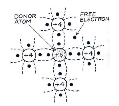
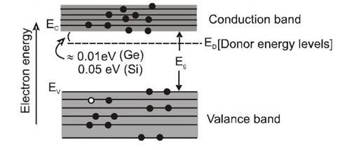
The fifth valence electrons of the impurity atoms occupy some discrete energy levels just below the conduction band. These are called 'donor levels' and are only 0.01 eV below the conduction band in case of Ge , and 0.05 eV below in case of Si. Therefore, at room temperature, the "fifth" electrons of almost all the donor atoms are thermally excited from the donor levels into the conduction band, where they move as charge-carriers when an external electric field is applied.
At ordinary temperature, almost all the electrons in the conduction band come from the donor levels; only a few come from the valence band. Therefore, the main charge carriers responsible for conduction are the electrons contributed by the donors. Since the excitation from the valence band is small, there are very few holes in this band.
The current contribution of the holes is, therefore small. Thus, in an n-type semiconductor, the electrons are the 'majority carriers' and the holes are the 'minority carriers.'
Some important facts about N-Type Semiconductor
These are obtained by adding a small amount of pentavalent impurity to a pure sample of semiconductor (Ge).
(1) Majority charge carriers - electrons Minority charge carriers - hole
Neutral
(2)
;
(3) Conductivity
(4) Donor energy level lies just below the conduction band.
(5) Electrons and hole concentration: In a doped semiconductor, the electron concentration
and the hole concentration
are not equal (as they are in an instrinsic semiconductor). It can be shown that
where
is the intrinsic concentration.
In an n-type semiconductor, the concentration of electrons in conduction band is nearly equal to the concentration of donor atoms
and very large compared to the concentration of holes in valence band. That is :
(6) Impurity atom called donar atom which is elements of V group of periodic table.
(7) Net charge on
type crystal is zero.
(8) Immobile charge is positive charge
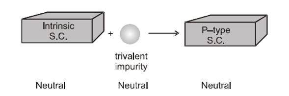
P-type semiconductor
When a trivalent impurity atom (boron, aluminium, gallium or indium) is added to a Ge (or Si ) crystal, it also replaces one of the Ge (or Si ) atoms in the crystal lattice. Its three valence electrons form covalent bonds with one each valence electron of these Ge (or Si ) atoms surrounding it. Thus, there remains an empty space, called a 'p-type' semiconductor because it has an excess of positive 'acceptor' atoms because they create holes which accept electrons.

The impurity atoms occupy vacant discrete energy levels just above the top of the valence band. These are called 'acceptor levels'. At room temperature, electrons are easily excited from the valence band into the acceptor levels. The corresponding holes created in the valence band are the main charge-carries in the crystal when an electric field is applied.
Thus, in a p-type semiconductor the holes are the 'majority carriers' and the few electrons, thermally excited from the valence band into the conduction band, are 'minority carriers'.
The adjacent figure shows Electron and hole concentrations for p-type semiconductor at T>0 K.
One thermally generated electron-hole pair + seven holes due to acceptor atoms.

Some important facts about P-Type Semiconductor
There are obtained by adding a small amount of trivalent impurity to a pure sample of semiconductor (Ge).
(1) Majority charge carries - holes
Minority charge carries – electrons
(2)
;
(3) Conductivity
(4) P-type semiconductor is also electrically neutral (not positively charged)
(5) Impurity is called Acceptor impurity which is element of III group of the periodic table.
(6) Acceptor energy level lies just above the valency band.
(7) Electron and hole concentration : In a p-type semiconductor, the concentration of holes in valence band is nearly equal to the concentration of acceptor atoms (
) and very large compared to the concentration of electron in conduction band. That is
(8) Net charge on p-type crystal is zero.
(9) Imobile charge is negative charge.
Distinction between intrinsic and extrinsic semiconductors
| Instrinsic Semiconductor |
Extrinsic Semiconductor |
| It is a pure, natural semiconductor, such as pure Ge and pure Si. |
It is prepared by adding a small quantity of impurity to a pure semiconductor, such as n-and p-type semiconductors. |
| In it the concentration of electrons and holes are equal. |
In it the two concentrations are unequal. There is an excess of electrons in n-type semiconductors and an excess of holes in p-type semiconductors. |
| Its electrical conductivity is very low. |
Its electrical conductivity is significantly high. |
| Its conductivity cannot be controlled. |
Its conductivity can be controlled by adjusting the quantity of the impurity added. |
| Its conductivity increases exponentially with temperature. |
Its conductivity also increases with temperature, but not exponentially. |
Distinction between -type and -type semiconductor :
| n-type semiconductor |
p-type semiconductor |
| It is an extrinsic semiconductor obtained by adding a pentavalent impurity to a pure intrinsic semiconductor. |
It is also an extrinsic semiconductor obtained by adding a trivalent impurity to a pure intrinsic semiconductor. |
| The impurity atoms added provide extra free electrons to the crystal lattice and are called donor atoms. |
The impurity atoms added create holes in the crystal lattice and are called acceptor atoms because the created holes accept electrons. |
| The electrons are majority carriers and the holes are minority carriers. |
The holes are majority carriers and the electrons are minority carriers. |
| The electron concentration is much more than the hole concentration. . |
The hole concentration is much more than the electron concentration . |
Electrical conductivity of extrinsic semiconductors
A semiconductor, at room temperature, contains electrons in the conduction band and holes in the valence band. When an external electric field is applied, the electrons move opposite to the field and the hole move in the direction of the field, thus constituting current in the same direction. The total current is the sum of the electron and hole currents.
Let us consider semiconductor block of length I, area of cross-section A and having electrons concentration
and hole concentration
.
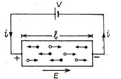
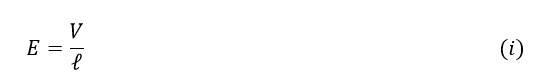
A potential difference applied across the ends of the semiconductor creates an electric field given by :
Under the field E, the electrons and the holes both will drift in opposite directions and constitute currents and respectively in the direction of the field. The total current flowing through the semiconductor is,
If
, be the drift velocity of the electrons in the conduction band and the drift velocity of the holes in the valence band, then we have
where is the magnitude of electron charge
Let R be the resistance of the semiconductor block and ![]() the resistivity of the block material.
the resistivity of the block material.
Then

Dividing eq.(i) by eq.(ii) we have
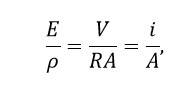
Because (Ohm's law). Substituting in it the value of i/A from eq.(ii), we get
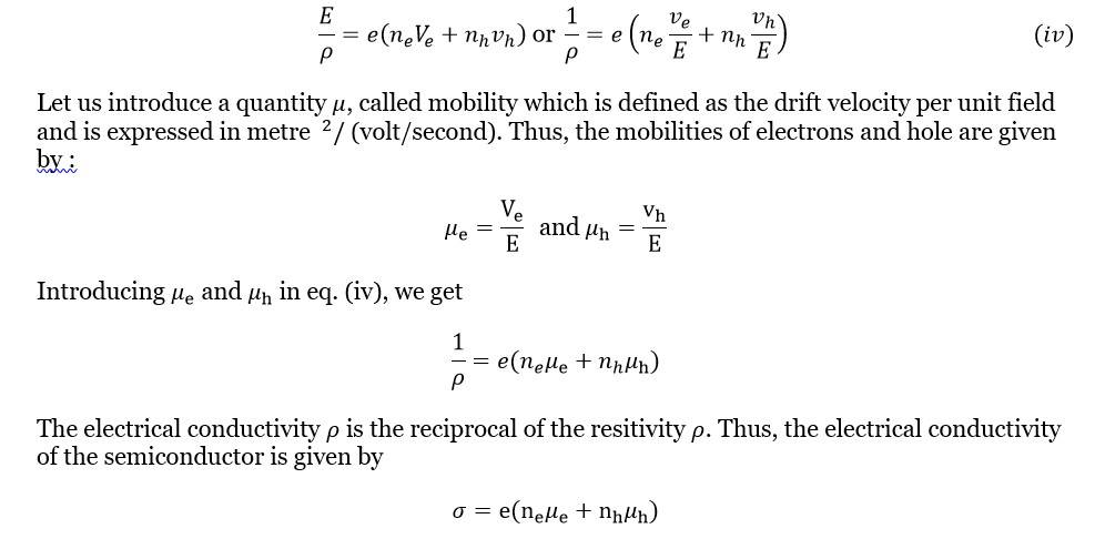
This is the required expression which proves that the electrical conductivity of a semiconductor depends upon the electron and hole concentrations (number densities) and their mobilities. The mobility of electrons is higher than the hole mobility.
Extrinsic Semiconductor Equations
About the Reviewer
Physics Semiconductor Devices Exam
Student Forum
Other Class 12th Physics Chapters
- Physics Alternating Current
- Physics Ray Optics and Optical Instruments
- Physics Electromagnetic Induction
- Physics Dual Nature of Radiation and Matter
- Physics Semiconductor Devices
- Physics Wave Optics
- Physics Current Electricity
- Physics Nuclei
- Physics Electrostatic Potential and Capacitance
- Physics Atoms
- Physics Moving Charges and Magnetism
- NCERT Class 12 Notes
- NCERT Class 12 Physics
- Physics Electric Charge and Field
- Physics Electromagnetic Waves
- Physics Magnetism and Matter