 / Preparation Physics Semiconductor Devices
Semiconductor Diode is basically a p-n junction that allows the flow of current in one direction (unidirectional flow). This device works on the principle of forward biased and reversed bias. The current can flow in forward bias while, in reverse bias it is blocked. Semiconductor diodes are used in rectifiers (AC to DC conversion), over voltage protection, signal demodulation, voltage regulation, and light sources (LEDs). Common types of semiconductor diodes are Zener diode, Schottky diode, Photodiode, and Tunnel diode. Through Semiconductor Diode Class 12 notes, students will know the definition of semiconductor diode, working principle of semiconductor diode under forward bias and reverse bias.
Semiconductor Diode is a key topic of Class 12 Physics Chapter 14 Semiconductor Electronics: Materials, Devices, and Simple Circuits. Mastering the topic will be helpful to the students preparing for the CBSE board exam and entrance test such as JEE Main / NEET.
The subject experts at Shiksha have uploaded the Class 12 Physics Chapter 14 NCERT solutions for intext and exercises problems. Students can use the NCERT Solutions for Clas 12 Physics to prepare for the test. Moreover, practicing the NCERT Solutions pdf will help to identify the important topics.
- Working Principle of Semiconductor Diode
- Types of Semiconductor Diode
- Example of Semicondcutor Didode
Working Principle of Semiconductor Diode
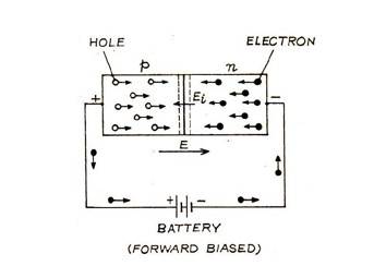
The working principle of semiconductor diode is based on p-n junction.The one side of junction is p-type and other is n-types. The p-type region contains holes (excess positive charge) while, n-types region is contains electrons (excess negative charge carriers). When an external voltage is connected to the p-n junctions, holes difuses from the p-type and electrons from n-type region. During the movement of charges a depletion region is formed at junction. This region creates an emf (internal electric field) that opposes the further flow of charges.
The behaviour of the diode depends on the polarirty: in forwards bias, barrier is reduced and allow the flow of current in one direction. While in reverse bias, barrier is widen which prevent the flow of current. Below is the detailed explanation of Semiconductor diode working priciple in forward bias and reverse bias.
Forward Biasing
In formaward biasing, external voltage is connected to the p-n junction in such that -region is connected to the positive terminal and -region is connected to the negative terminal as shown in the figure.
Forward-Biased Characteristics:
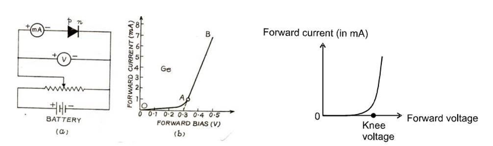
In the circuit connection setup (as shown in the figure), p-n diode is connected through a potential-divider arrangement which enables to change the applied voltage. The voltage across the diode is measured through voltmeter (V) while, millimeter (mA) measure the current.

- In the forward bias current is increased from a low value.
- The corresponding current is noted.
- A graph is then plotted between voltage and current, resulting curve OAB is the forward characteristic of the diode.
Behaviour:
- Initially, the current through the diode is almost zero (0) due to potential barrier (about 0.3 V for junction and about 0.7 V for the Si junction).
- When the applied voltage is increased, current increases slowly and non-linearly until the voltage exceeds the potential barrier (curve OA).
- Current increases rapidly and alomost linearly (line AB) beyond barrier voltage, this indicates diode now behave like an ordinary conductor.
- This is represented by the straight-line part of the characteristic. If this straight line is projected back. It intersects the voltage axis at the barrier potential voltage.
Note :
(i) The depletion layer decreases in forward bias.
(ii) The resistance offered in the forward bias is
(iii) Forward bias opposes the potential barrier and for
a forward current is set up across the junction.
(iv) Cut-in (Knee) voltage: The voltage at which the current starts to increase rapidily (≈ 0.3 V for Ge, ≈ 0.7 V for Si).
Reverse Biasing
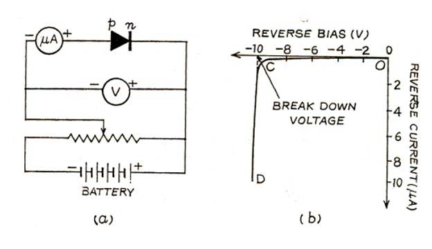
A junction diode is reverse-biased when the positive terminal of the external battery is connected to the n-region and the negative terminal to the p -region of the diode (Fig.). This confiuration of diode causes depletion region to widen the barrier and prevent the flow of current.
Reversed Biased Characteristics
In reverse biased junction, a very small current flow across the junction due to the motion of the few thermally-generated minoritiy carriers (electrons in the p-region and holes in the n-region).
The small reverse current remains almost constant over a sufficiently long range of reverse bias (applied voltage), increasing very little with increasing bias. This is represented by the part OC of the reverse characteristic curve (Fig b).
Note:
(i) The depletion layer increases in reverse bias.
(ii) Resistance offered in reverse biased
(iii) Reverse bias supports the potential barrier, preventing the current flow.
(iv) A small reverse current exist due to the drifting of minority carriers across the junction)
(v) Break down voltage: Reverse voltage at which semiconductor breaks down occurs ( For Ge it is 25 V and for Si it is 35 V).
Types of Semiconductor Diode
Below is the types of semiconductor alongwith their applications.
| Types of Semiconductor Diode | Applications |
| Zener Diode | Stabilisation of current and voltage |
| Rectifier Diode | Retification of AC to DC |
| Photodiode | Work as photo detector |
| Tunnel Diode | Used in negative dynamic resistance region |
| Switching Diode | Fast switching of electrical signals |
| Variable capacitance diode | Used in reversed biased |
| LED | Emitting infrared light spectrum |
Example of Semicondcutor Didode
The semiconductor is a material that allows the flow of current within it. Silicon is the most commonly used material in the semiconductor. Below are the examples of semiconductors and their uses.
Examples of Semiconductors:
- Silicon (Si): Used in solar cells, transistors and microchips.
- Gallium Arsenide (GaAs): Used in laser diode, microwave integrated circuits, and high-speed electronics.
- Gallium Nitride (GaN): Used in high-frequency devices and power electronics
- Germanium (Ge): Used in infrared detectors.
- Indium Phosphide (InP): Used in optoelectronics and high-speed electronics.
- Zinc Oxide (ZnO): Used in solar cells, sensors and various applications.
Physics Semiconductor Devices Exam
Student Forum
Other Class 12th Physics Chapters
- Physics Alternating Current
- Physics Ray Optics and Optical Instruments
- Physics Electromagnetic Induction
- Physics Dual Nature of Radiation and Matter
- Physics Semiconductor Devices
- Physics Wave Optics
- Physics Current Electricity
- Physics Nuclei
- Physics Electrostatic Potential and Capacitance
- Physics Atoms
- Physics Moving Charges and Magnetism
- NCERT Class 12 Notes
- NCERT Class 12 Physics
- Physics Electric Charge and Field
- Physics Electromagnetic Waves
- Physics Magnetism and Matter