 / Preparation Physics Semiconductor Devices
Semiconductor is a material whose electrical conductivity lies between a conductor and an insulator. Semiconductor has the properties of both a conductor as well as an insulator. To change the conductivity of a semiconductor, a specific number of impurities are added through the process called doping. Moreover, the conductivity of a semiconductor can also be affected by external factors such as temperature and electric field.
Semiconductors are categorised into two types:
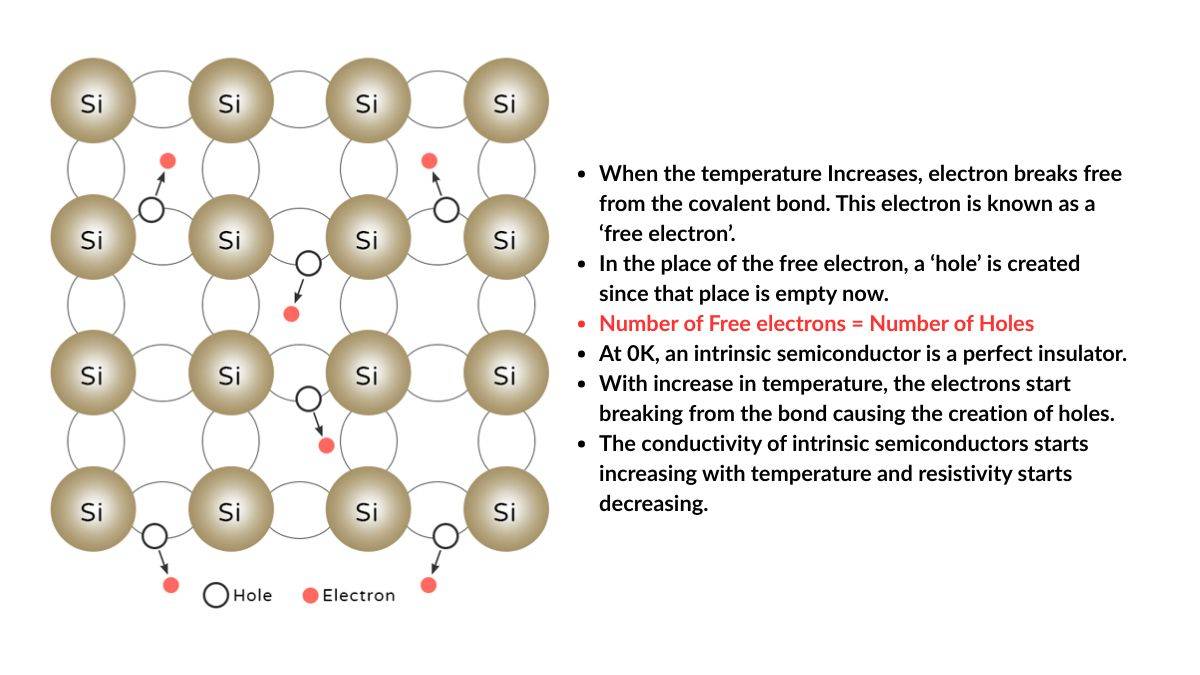
Intrinsic Semiconductors: These are considered to be pure semiconductors; in other words, free from impurities. This means the number of electrons and holes is the same. Moreover, an Intrinsic semiconductor acts as an insulator when T = 0 K. Silicon (Si) and Germanium (Ge) are examples of Intrinsic semiconductors.
Extrinsic Semiconductors: Intrinsic semiconductor conductivity depends on temperature, but at room temperature, its conductivity is very low. Due to this, it is difficult to use intrinsic semiconductors in many electronic devices. To increase the conductivity of the semiconductor, a small amount of suitable impurities is added to the pure semiconductor. Such semiconductors are called extrinsic or impure semiconductors.
- N-type Semiconductor: Pure semiconductors have limited electrons, due to which they are not considered a good conductor. Doping pentavalent impurities such as phosphorus, arsenic, or antimony increases the number of free electrons, which makes the n-type semiconductor a good conductor. Pentavalent elements have five valance electron. In the crystal lattice, when a pentavalent atom replaces the silicon atoms, four valence electrons form bonds with the silicon atoms, leaving one electron free. The "n" in n-type semiconductor refers to the negative electron.
- P-type Semiconductor: In a p-type semiconductor, holes are the majority charge carrier. Doping of an intrinsic semiconductor like silicon with a trivalent impurity such as boron, aluminium, or indium introduces holes in the crystal lattice. These holes acts as positive charge carrier.
- Classification of Metals, Conductors and Insulators
- Semiconductor
- Conductors
- Insulator
- Types of Semiconductor Devices
- Working Principle of Semiconductor Device
- Energy Levels and Energy Bands in Solids
- Energy Bands
- Energy Band Description of Conductor, Insulator and Semiconductor
- Conduction band and valence band in monovalent metal
- Conduction band and valence band in bivalent metal
- Examples of Semiconductor Devices
- Semiconductor Device Questions for JEE Mains and NEET
- Practical Application of Semiconductor Device
Classification of Metals, Conductors and Insulators
On the basis of conductivity: On the basis of the relative values of electrical conductivity ( ) or resistivity ( ), the solids are broadly classified as:
(i) Metals: They possess very low resistivity (or high conductivity).
(ii) Semiconductors: They have resistivity or conductivity intermediate to metals and insulators.
(iii) Insulators: They have high resistivity (or low conductivity).
The values of
and
given above are indicative of magnitude and could well go outside the ranges as well. Relative values of the resistivity are not the only criteria for distinguishing metals, insulators and semiconductors from each other. There are some other differences, which will become clear as we go along in this chapter. Our interest in this chapter is in the study of semiconductors which include:
(i) Elemental semiconductors: Si and Ge
(ii) Compound semiconductors: Examples are:
- Inorganic: CdS, GaAs, CdSe, InP, etc.
- Organic: anthracene, doped pthalocyanines, etc.
- Organic polymers: polypyrrole, polyaniline, polythiophene, etc.
Most of the currently available semiconductor devices are based on elemental semiconductors Si or Ge and compound inorganic semiconductors. However, after 1990, a few semiconductor devices using organic semiconductors and semiconducting polymers have been developed signalling the birth of a futuristic technology of polymerelectronics and molecular-electronics. In this chapter, we will restrict ourselves to the study of inorganic semiconductors, particularly elemental semiconductors Si and Ge . The general concepts introduced here for discussing the elemental semiconductors, by-and-large, apply to most of the compound semiconductors as well.
Semiconductor
A Semiconductor is device that allows the flow of current through it but it is neither a conductor nor an insulator. Examples of semiconductor devices are transistors, Diode, ICs etc. The identification of a semiconductor device is based on the Lattice structure and the atomic structure of constituent elements. Semiconductors are elemental (Si, Ge) as well as compound (GaAs, CdS, etc).
Physics Semiconductor Devices are classified as two-terminal, three-terminal and four-terminal. The example of a few semiconductor devices is transistors, diodes, Integrated Circuits (ICs), Photonic Devices, sensors and detectors, etc. Through this article, we will learn about energy levels and energy bands in solids, conductors, insulators and various applications of semiconductor devices.
Conductors
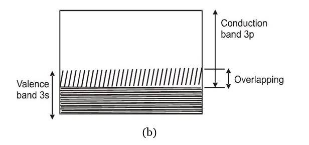
These are solids in which either the energy band containing valence band is partially filled or the energy band containing valence electrons overlaps with next higher band to give a new band which is partially filled too. For both these situations there are enough free levels available for electrons to which they can be excited by receiving energy from an applied electric field.
Insulator
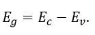
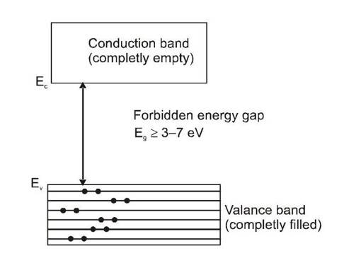
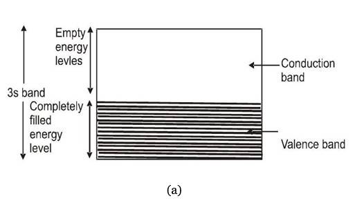
It is a solid in which the energy band formation takes place in such a manner, that the valence band is completely filled while the conduction band is completely empty. In addition to this, these two bands are separated by a large energy gap called forbidden energy gap or band gap. If and respectively denotes the minimum energy in conduction band and the maximum energy in valence band then band gap is defined as
For insulators to 7 eV . As in an empty band no electron is there to take part in the process of electric conduction, such a band does not contribute in conduction. In a completely filled band very large number of electrons are present but no vacant levels to which these electrons make transition are available and hence again there will not be any conduction.
As explained earlier ordinary current sources provide only a very small energy to an electron in a solid and so electrons cannot be excited from valence band to conduction band. Also not only at ordinary temperatures but at elevated temperatures too, the thermal energy is much smaller than the band gap energy
so electrons cannot be excited from valence band to conduction band by thermal means. Consequently solids with such large band gaps are insulators.
For diamond,
hence it is insulator.
In general electrical conductivities of insulators are in the range metre to (resitivity in the range ohm-metre to ohm metre.]
Types of Semiconductor Devices
Semiconductor devices are classified in three categories:
Two terminals - This terminal is capable of transmitting the current in a single direction. It is the combination of positive (p) and negative (n) (p-n junctions). Examples of a two-terminal semiconductor are a diode, a laser diode, Zener diode, a Light-emitting diode (LED), Photocell, a Phototransistor, Solar cell, etc.
Three terminals - These types of semiconductors can control the flow of current by turning it on and off. Examples of a terminal semiconductor are Silicon-controlled rectifier, TRIAC, Thyristor, Bipolar transistor, IGBT, Field-effect transistor, etc.
Working Principle of Semiconductor Device
The working of Semiconductors depends on the movement of electrons and holes. The electrical conductivity of a semiconductor is not fixed; however, it is based on temperature, impurities (doping), and applied voltage.
A pure semiconductor (Silicon (Si) and germanium (Ge)) behaves as an insulator at absolute zero (0) temperature. When the temperature rises, the electrons easily flow from the valence band to the conduction band, allowing current to flow.
Energy Levels and Energy Bands in Solids
The electrons of an isolated atom are restricted to well defined energy levels. The maximum number of electrons which can be accommodated in any level is determined by the Pauli exclusion principle. The electrons belonging to the outermost energy level are called valence electrons. For example, the
electronic configuration of sodium (atomic number 11) is
, here the electron belonging to the
level is the valence electron. Most of the solids including metals with which we are familiar occur in crystalline form. As we know a crystal is a regular periodic arrangement of atoms separated from each other by very small distance called lattice constant. The value of lattice constant is different for different crystalline solids, however it is of the order of linear dimension of atoms
. Obviously at such a short separation between various neighbouring atoms, electrons in an atom cannot only be subjected to the Coulombic force of the nucleus of this atom but also oby Coulombic forces due to nuclei and electrons of the neighbouring atoms. In fact it is this interaction which results in the bonding between various atoms which leads to the formation of crystals.
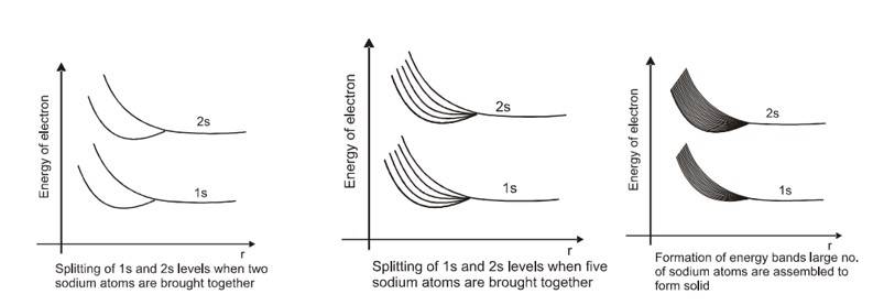
When atoms are interacting (such as in crystal) then the energy level scheme for the individual atoms as shown in figure(a) does not quite hold. The interaction between atoms affect the electron energy levels, as a result there occurs a splitting of energy levels belonging to various atoms. To understand this phenomenon in more clear terms, let us first consider the simplest case of two interacting identical atoms. Let us assume that initially they are far apart i.e. the forces of interaction between them can be neglected. [If the distance between two atoms is much larger (
) compared to their linear dimensions (
) this assumption is reasonably correct] .In such a case we may treat them as isolated with energy levels like that for the case of an isolated atom as shown in figure(a).
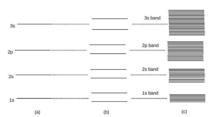
In crystals the number of atoms, N is very large of the order of to per cubic centimetre, so each energy band contains as many levels as the number of atoms. The spacing between various levels within a band is therefore very small. If for example we assume the total width of a band of energies as 1 eV and levels are to be accommodated with in this band, then the average spacing between the adjacent levels is about . For all practical purposes, therefore, energy within a band can be assumed to vary continuously. The formation of bands in a solid is shown schematically in figure (c).
Energy Bands
Energy Band Description of Conductor, Insulator and Semiconductor
Conduction band and valence band in monovalent metal
Conduction band and valence band in bivalent metal
Examples of Semiconductor Devices
Semiconductor Device Questions for JEE Mains and NEET
Practical Application of Semiconductor Device
Physics Semiconductor Devices Exam
Student Forum
Other Class 12th Physics Chapters
- Physics Alternating Current
- Physics Ray Optics and Optical Instruments
- Physics Electromagnetic Induction
- Physics Dual Nature of Radiation and Matter
- Physics Semiconductor Devices
- Physics Wave Optics
- Physics Current Electricity
- Physics Nuclei
- Physics Electrostatic Potential and Capacitance
- Physics Atoms
- Physics Moving Charges and Magnetism
- NCERT Class 12 Notes
- NCERT Class 12 Physics
- Physics Electric Charge and Field
- Physics Electromagnetic Waves
- Physics Magnetism and Matter