 / Preparation Physics Semiconductor Devices
A diode is an electronic device that allows the flow of current in only one direction. Due to this property, it is known as a rectifier. This means a circuit that converts AC to DC.
Direct Current (DC) is used in everyday life. Some electronic devices, like mobile chargers, radios, and laptops, require DC to work. The electricity from the power outlet is AC. When we use a diode as a rectifier, it plays an important role by acting as a bridge to change AC into DC.
In this article, students will learn about AC to DC conversion, half-wave and full-wave rectification, bridge rectifier circuit, output waveform, forward and reverse bias, and load resistance.
Students can refer to the Class 12 Chapter 14 Semiconductor Electronics NCERT solutions for in-text and exercise problems. NCERT Class 12 Physics solutions are a useful resource for the preparation of the CBSE board exam and competitive exams such as JEE Main, NEET, etc. Practising the NCERT solutions will help to develop a good command of the topics and identify the important questions.
- Working Principle of Diode as Rectifier
- Different Types of Junction Diode
- Junction Transistor
- Common Emitter (CE), Common Base (CB), Common Collector (CC). Working of Transistor
- Transistor Configurations
- Feedback amplifier and transistor oscillator :
- Analogue Circuits and Digital Circuits and signal :
- Example of Rectifier
Working Principle of Diode as Rectifier
Here we will discuss the working principle of a Diode as a rectifier in full wave and half wave.
Half-Wave Rectifier
The half-wave rectifier circuit is shown in Fig. (a) and the input and output wave forms in Fig. (b).
- The alternating input voltage is applied across the primary of a transformer.
- It is the secondary coil of the same transformer. is connected to the p-type crystal of the junction diode and is connected to the n-type crystal through a load resistance .
- During the first half-cycle of the a.c. input, when the terminal of the secondary is positive and is negative, the junction diode is forward-biased.
Hence it conducts and current flows through the load in the direction shown by arrows. The current produces across the load an output voltage of the same shape as the half-cycle of the input voltage.
During the second half-cycle of the a.c. input, the terminal is negative and is positive. The diode is now reverse-biased. Hence there is almost zero current and zero output voltage across . The process is repeated. Thus, the output current is unidirectional, but pulsating, as shown in the lower part of Fig. (b).
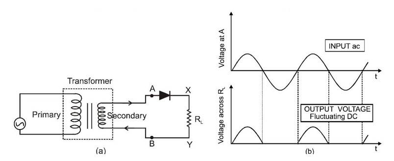
Since the output current corresponds to one-half of the input voltage wave, the other half being missing, the process is called half-wave rectification.
The purpose of the transformer is to supply the necessary voltage to the rectifier. If direct current at high voltage is to be obtained from the rectifier, as is necessary for power supply, then a step-up transformer is used, as shown in Fig. (a). In many solid-state equipment, however, a direct current of low voltage is required. In that case, a step-down transformer is used in the rectifier.
Note :
(i) During the positive half cycle
Diode
forward biased
Output signal
obtained
(ii) During negative half cycle
Diode
reverse biased
Output signal
not obtained
(iii) Output voltage is obtained across the load resistance
. It is not constant but pulsating (mixture of ac and dc) in nature.
(iv) r.m.s. output:
(v) Efficiency is
(vi) The ripple frequency (
) for a half-wave rectifier is the same as that of ac.
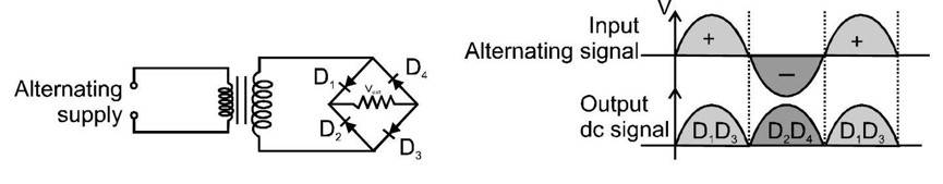
p-n Junction Diode as Full-Wave Rectifier
In a full-wave rectifier, a unidirectional, pulsating output current is obtained for both halves of the alternating input voltage. Essentially, it requires two junction diodes so connected that one diode rectifies one half and the second diode rectifies the second half of the input.
The circuit for a full-wave rectifier is shown in Fig. (a) and the input and output wave forms in Fig. (b).
- The alternating input voltage is applied across the primary of a transformer.
- The terminals and of the secondary are connected to the p-type crystals of the junction diodes and whose n-type crystals are connected.
- Load resistance
is connected across the n-type crystals and the central tap T of the secondary
.
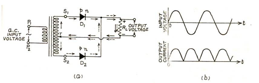
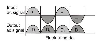
During the first half-cycle of the a.AC the input voltage, the terminal is suppose positive relative to and is negative. In this situation, the junction diode is forward-biased and is reverse-biased. Therefore, conducts while does not. The conventional current flows through diode load and the upper half of the secondary winding, as shown by solid arrows. During the second half-cycle of the input voltage, is negative relative to and is positive. Now, is reverse-biased and does not conduct while is forward-biased and conducts. The current now flows through , the load and the lower half of the secondary, as shown by dotted arrows. It may be seen that the current in the load flows in the same direction for both half-cycles of the alternating input voltage.
Thus, the output current is a continuous series of unidirectional pulses. However, it can be made fairly steady by means of smoothing filters.
Filter: The rectified voltage is in the form of pulses in the shape of half sinusoids. Though it is unidirectional it does not have a steady value. To get steady dc output from the pulsating voltage normally a capacitor is connected across the output terminals (parallel to the load
). One can also use an inductor in series with
for the same purpose. Since these additional circuits appear to filter out the AC ripple and give a pure DC voltage, they are called filters.
Now we shall discuss the role of capacitors in filtering. When the voltage across the capacitor is rising, it gets charged. If there is no external load, it remains charged to the peak voltage of the rectified output. When there is a load, it gets discharged through the load and the voltage across it begins to fall. In the next half-cycle of rectified output, it again gets charged to the peak value. The rate of fall of the voltage across the capacitor depends upon the inverse product of capacitor
and the effective resistance Rı used in the circuit and is called the time constant. To make the time constant large value of
should be large. So capacitor input filters use large capacitors. The output voltage obtained by using a capacitor input filter is nearer to the peak voltage of the rectified voltage. This type of filter is most widely used in power supplies.
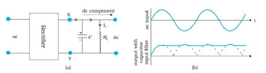
FIGURE (a) A full-wave rectifier with capacitor filter, (b) Input and output voltage of rectifier in(a). NOTE :
(i) During the positive half cycle
Diode:
forward biased
reverse biased
Output signal
obtained due to
only
(ii) During negative half cycle
Diode:
reverse biased
forward biased
Output signal
obtained due to
only
(iii) Fluctuating dc
Filter
constant dc.
(iv) Output voltage is obtained across the load resistance RL. It is not constant but pulsating in nature.
(v) Average output:
(vi) Ripple frequency: The ripple frequency of full wave rectifier
(Frequency of input ac)
(vii) Efficiency = 81.2%
Full wave bridge rectifier: Four diodes and are used in the circuit. During the positive half cycle and are forward biased and are reverse biased. During the negative half cycle and are forward biased and and are reverse biased.
Different Types of Junction Diode
The junction diodes are of many types. The important types are Zener diode, photodiode, light-emitting diode (LED) and solar cell.
(i) Zener Diode: It is a voltage-regulating device based upon the phenomenon of avalanche breakdown in a junction diode.
When the reverse bias applied to a junction diode is increased, there is an abrupt rise in the (reverse) current when the bias reverse reaches a certain value, known as 'breakdown voltage' or 'Zener voltage'.
Thus, in this region of the reverse characteristic curve, the voltage across the diode remains almost constant for a large range of currents. Hence, the diode may be used to stabilize voltage at a pre-determined value. It is then known as a 'Zener diode'. It can be designed, by properly controlled doping of the diode, to stabilise voltage at any desired value between volt. Fig. (a) shows the symbol of a Zener diode, and Fig. (b) shows a simple circuit for stabilizing the voltage across a load RL. The circuit consists of a series voltage-dropping resistance R and a Zener diode in parallel with the load .
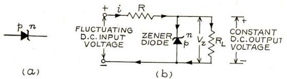
The diode is selected with a Zener voltage equal to the desired voltage across the load. The fluctuating d.c. input voltage may be the d.c. output of a rectifier.
An increase in the input voltage results in a drop in the excess voltage across the resistance R. It thus increases the input current
. This increase is conducted by the Zener diode, while the current through the load and hence the voltage across it remains constant at Vz. Similarly, whenever, input voltage is decreased, causes a decrease in the input current i . The current through the diode decreases correspondingly, again maintaining the current through the load constant.
Since the resistance R absorbs the input voltage fluctuations to give a constant output voltage
, the circuit cannot work if the input voltage falls below
.
(ii) Photodiode: A photodiode is a reverse-bias p-n junction made from a photosensitive semiconductor. The junction is embedded in clear plastic. The upper surface across the junction is open to light, while the remaining sides of the plastic are painted black or enclosed in a metallic case. The entire unit is extremely small, of the order of 0.1 inch in size.
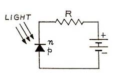
The absence of light in junction and the reverse bias is of the order of a few tenths of a volt, and an almost constant small current
is obtained. This "dark" current is referred to as reverse saturation current due to the thermally-generated minority-carriers (electrons in the p-region and holes in the n-region). When light of appropriate frequency is made incident on the junction, additional electron-hole pairs are created near the junction (due to the breaking of covalent bonds). The light-generated minority-carriers cross the (reverse-bias) junction and contribute to the (reverse) current due to thermally generated carriers. Therefore, the current in the circuit increases (a fraction of a mA). This so-called 'photoconductive' current varies almost linearly with the incident light flux.
The p-n photodiodes are capable of operating at frequencies of the order of 1 MHz. It is commonly used in high-speed reading of computer punched cards, light-detection systems, light-operated switches, electronic counters, etc.
(iii) Light-Emitting Diode (LED): Operates in forward-bias. The movement of electrons and the holes is towards the junction. As they cross the junction, the electrons fall into the holes (recombine), which releases the energy at the junction (because the electrons fall from a higher to a lower energy level). The energy released is infrared radiation.
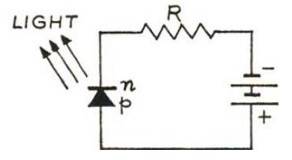
In case the diode is made of gallium arsenide or indium phosphide, and the energy released is visible light. Then the junction is referred to as a 'light-emitting diode' (LED).
The incandescent lamps are replaced by LEDs due to their low input power, long life and fast on-off switching. Light Emitting Diodes are used in fancy electronic devices like calculators etc.
Junction Transistor
Transistor structure and action :
A transistor comprises a semiconductor device with two p-n junctions, formed by three doped regions. There are two types of transistors, as shown in the figure.
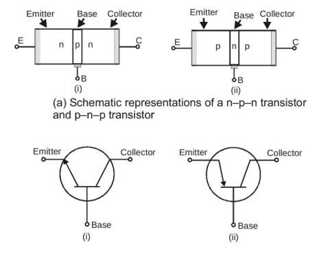
(b) Symbols for n-p-n and p-n-p transistors.
- n-p-n Transistor: Consists of two n-type regions, the emitter and the collector, with a p-type region, the base, in between.
- p-n-p Transistor: Composed of two p-type regions, the emitter and the collector, with an n-type base in between.
The n-p-n and a p-n-p configuration are represented in the figure. Transistors are divided into three parts of different doping concentration and thickness:
- Emitter: Mostly doped to inject large amounts of charge carriers.
- Base: Very thin and lightly doped so that most of the carriers can pass through.
- Collector: Moderately doped and of a larger size. This enables efficient heat dissipation.
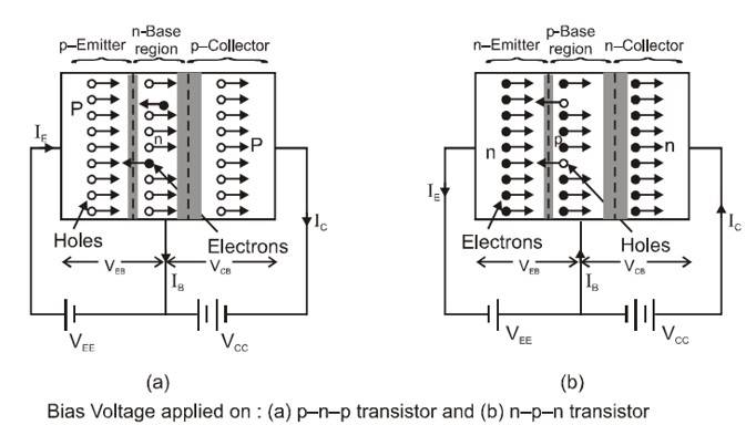
As compared to a single p-n junction diode, a transistor generates two depletion regions: one at the emitter-base junction and the other at the base-collector junction.
Biasing and Active Mode
The transistor is operatively functioning in the active region in terms of amplification for which:
- The emitter-base junction is forward-biased.
- The collector-base junction is reverse-biased.
This arrangement enables efficient current flow from the emitter to the collector. The associated voltages are:
- VEB: Voltage at the emitter terminal and the base.
- VCB: Voltage at the collector terminal and the base.
In this arrangement, the base is a common point to both sides (power sources) and therefore serves as a dual terminal.
Movement of carrier and current
In a p-n-p transistor:
- The emitter injects holes into the base.
- The base is very thin and only lightly doped, so most holes cross over to the collector instead of recombining in the base.
- These holes are attracted to the collector which is reverse-biased.
Of the total base current supplied, only a small portion of the emitter current becomes base current, the remaining part serves to increase the collector current. This is described mathematically as:
The flow of conventional current is associated with the movement of holes, but it works against electron movement. In p-n-p transistors, current flows out from the emitter to the base, and in n-p-n types, it flows in from the base to the emitter.
Common Emitter (CE), Common Base (CB), Common Collector (CC). Working of Transistor
(1) There are four possible ways of biasing the two
junctions (emitter junction and collector junction) of transistor.
(i) Active mode : Also known as linear mode operation.
(ii) Saturation mode : Maximum collector current flows and transistor acts as a closed switch from collector to emitter terminals.
(iii) Cut-off mode : Denotes operation like an open switch where only leakage current flows.
(iv) Inverse mode : The emitter and collector are inter changed.
Different modes of operation of a transistor
| Operating mode |
Emitter base bias |
Collector base bias |
| Active |
Forward |
Reverse |
| Saturation |
Forward |
Forward |
| Cut off |
Reverse |
Reverse |
| Inverse |
Reverse |
Forward |
(2) A transistor is mostly used in the active region of operation i.e., emitter base junction is forward biased and collector base junction is reverse biased.
(3) From the operation of junction transistor it is found that when the current in emitter circuit changes. There is corresponding change in collector current.
(4) In each state of the transistor there is an input port and an output port. In general each electrical quantity (V or I) obtained at the output is controlled by the input.
Transistor Configurations
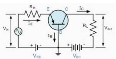
Each transistor has three terminals: Emitter (E), Base (B) and Collector (C). Depending on which terminal is common to both input and output, a transistor can be configured in:
(1) CB configurations: Base is common to both emitter and collector.
(i) Input current
(ii) Input voltage
(iii) Output voltage
(iv) Output current
With a small increase in emitter-base voltage
, the emitter current
increases rapidly due to small input resistance.
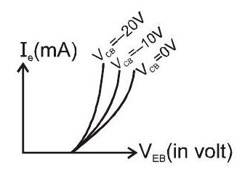
(v) Input characteristics: If
constant, the curve between
and
is known as input characteristics. It is also known as emitter characteristics:
Input characteristics of NPN transistors are also similar to the above figure but
and
both are negative and VCB positive. Dynamic input resistance of a transistor is given by
(vi) Output characteristics: Taking the emitter current
constant, the curve drawn between
and
are known as output characteristics of configuration.
Dynamics output resistance

Note: Transistor as CB amplifier
(i) AC gain
(ii) DC gain
or
value of
lies between 0.95 to 0.99
(iii) Voltage gain
(iv) Power gain
Power gain
Resistance gain
(v) Phase difference (between output and input): same phase
(vi) Application: For High frequency
COMMON EMITTER(CE): The transistor is most widely used in the CE configuration.
When a transistor is used in CE configuration, the input is between the base and the emitter and the output is between the collector and the emitter. The variation of the base current
with the base-emitter voltage
is called the input characteristic. The output characteristics are controlled by the input characteristics. This implies that the collector current changes with the base current.
CE configurations: Emitter is common to both base and collector.
The graphs between voltages and currents, when the emitter of a transistor is common to input and output circuits, are known as CE characteristics of a transistor.
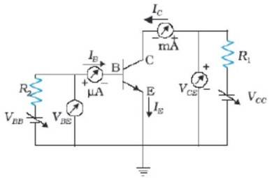
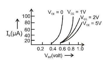
Input characteristics: The input characteristics curve is drawn between the base current and emitter-base voltage , at constant collector-emitter voltage .
Dynamic input resistance
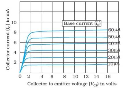
Output characteristics: Variation of collector current
with
can be noticed for
between 0 to 1 V only. The value of
up to which the Ic changes with
is called knee voltage. The transistor are operated in the region above knee voltage.
Dynamic output resistance
(b) Transistor as a device
The way a transistor works really hinges on its setup—like whether it’s in Common Base (CB), Common Collector and Common Emitter mode. It also depends on how the emitter-base (E-B) and base-collector (B-C) junctions are biased, along with the operational region: cutoff, active, or saturation.
- In the cutoff or saturation regions, the transistor acts like a switch.
- For it to serve as an amplifier, the transistor needs to be in the active region, where it can effectively manage and boost signals.
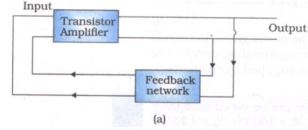
Feedback amplifier and transistor oscillator :
In an oscillator, we get AC output without any external input signal. A portion of the output power is returned back (feedback) to the input in phase with the starting power (this process is termed positive feedback) as shown in Figure (a). The feedback can be achieved by inductive coupling (through mutual inductance) or LC or RC networks.
Suppose switch is put on to apply proper bias for the first time. A surge of collector current flows in the transistor. This current flows through the coil where terminals are numbered 3 and 4 (Fig. b).

This current does not reach full amplitude instantaneously but increases from X To Y, as shown in figure(C). The inductive coupling between coil and coil now causes a current to flow in the emitter circuit (note that this is the 'feedback' from input to output). As a result of this positive feedback, this current (in emitter current) also increases from to Fig. (C) (ii).
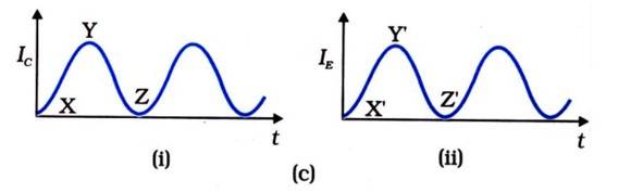
The current in (collector current), connected in the collector circuit acquires the value Y when the transistor becomes saturated. This means that the maximum collector current is flowing and can increase no further. Since there is no further change in collector current, the magnetic field around ceases to grow. As soon as the field becomes static, there will be no further feedback from to . Without continued feedback, the emitter current begins to fall. Consequently, the collector current decreases causing the magnetic field to decay around the coil . Thus, is now seeing a decaying field in (opposite from what it saw when the field was growing at the initial start of operation). This causes a further decrease in means that both and cease to flow. Therefore, the transistor has reverted back to its original state (when the power was first switched on). The whole process now repeats itself. The transistor is driven to saturation, then to cut-off, and then back to saturation. The time for a change from saturation to cut-off and back is determined by the constant of the tank circuit or tuned circuit (inductance of Coil and connected in parallel to it). The resonance frequency (v) of this tuned circuit determines the frequency at which the oscillator will oscillate.
Analogue Circuits and Digital Circuits and signal :
There are commonally two types of electronic circuits: Analogue circuits and Digital circuits:
Analogue circuits:
- Continuous variation in voltage (or current) with time (Figure A).
- Such a voltage signal is called an 'analogue signal'.
- The figure represents a typical voltage analogue signal varying sinusoidally between 0 and 5 V.
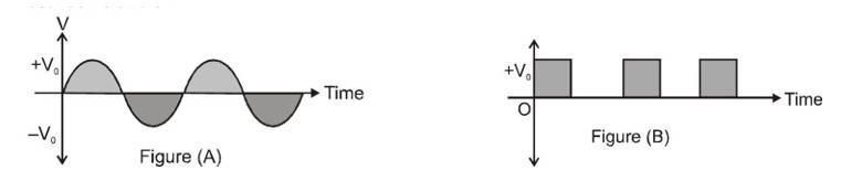
Digital circuits:
- The voltage has only two levels, either zero or some constant value of voltage (Figure B).
- A signal having only two levels of voltage (or current) is called a 'digital signal'.
- Figure shows a typical digital signal in which the voltage at any time is either 0 or 5 V.
- The binary number is used in the digital circuits, such that two levels of the (digital) signal are represented by the digits 0 and 1 only.
- The example of digital circuits are the basis of calculators, computers, etc.
Example of Rectifier
Physics Semiconductor Devices Exam
Student Forum
Other Class 12th Physics Chapters
- Physics Alternating Current
- Physics Ray Optics and Optical Instruments
- Physics Electromagnetic Induction
- Physics Dual Nature of Radiation and Matter
- Physics Semiconductor Devices
- Physics Wave Optics
- Physics Current Electricity
- Physics Nuclei
- Physics Electrostatic Potential and Capacitance
- Physics Atoms
- Physics Moving Charges and Magnetism
- NCERT Class 12 Notes
- NCERT Class 12 Physics
- Physics Electric Charge and Field
- Physics Electromagnetic Waves
- Physics Magnetism and Matter