 / Preparation Physics Semiconductor Devices
A semiconductor free from impurities is called an intrinsic semiconductor. This type of semiconductor has an equal number of electrons (in the excited state) and holes (n = p). It is also known as a pure semiconductor, i-type semiconductor or undoped semiconductor. Even if the semiconductor is doped, it can remain intrinsic in nature, but for this condition, the number of donors and acceptors should be equal. Silicon and Germanium are examples of intrinsic semiconductors.
- What is Intrinsic Semiconductor
- Intrinsic Semiconductor Definition
- Types of Intrinsic Semiconductor
- Class 12 Physics Notes on Intrinsic Semiconductor
- Working Principle of Intrinsic Semiconductor
- Difference Between Intrinsic and Extrinsic Semiconductors
- Intrinsic Semiconductor Equations
- Examples of Intrinsic Semiconductor
- Intrinsic Semiconductor Questions in JEE Main and NEET
- Frequently Asked Questions on Intrinsic Semiconductor
What is Intrinsic Semiconductor
A semiconductor free from impurities is called an intrinsic semiconductor. Every intrinsic semiconductor belongs to group 14 elements, and these only have 4 valence P electrons, which are available for bonding in their outermost shell. Ideally, an intrinsic semiconductor crystal should contain atoms of this semiconductor only but it is not possible in practice to obtain crystals with such purities. However if the impurity is less than 1 in
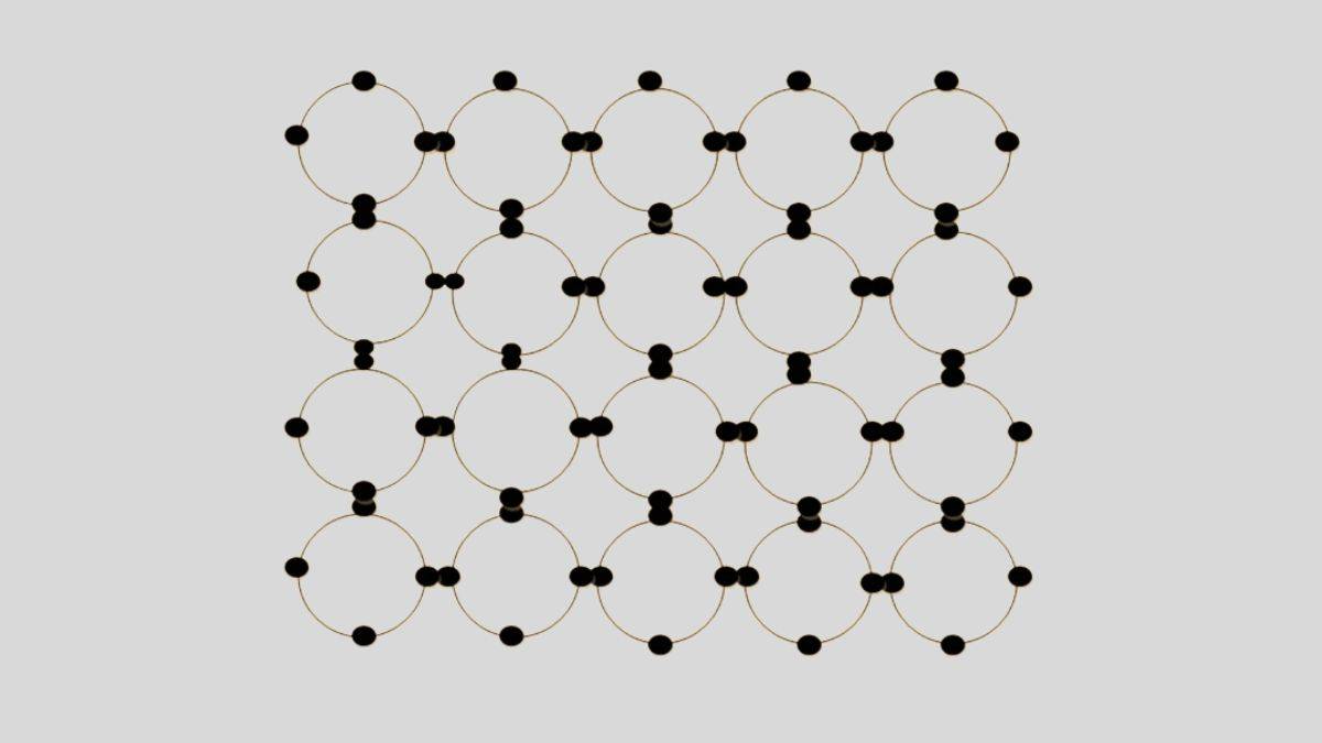
part of semiconductor it can be treated as intrinsic. This type of semiconductor has an equal number of electrons (in the excited state) and holes (n = p). Because of these 4 electrons, group 14 elements are able to form crystal lattice structures as shown below
Semiconductor Diagram
Below is the image of semiconductor with electrons and holes description.
Intrinsic Semiconductor Definition
"In intrinsic semiconductors, the number of free electrons, ne is equal to the number of holes, nh. That is
ne = nh = ni
where ni is called the intrinsic carrier concentration."
As explained above in the first section, definition of intrinsic semiconductor states that the number of holes created are equal to the number of free electrons released in the lattice. Both holes and electrons are the charge carriers, due to which the charge carrier concentration in an intrinsic semiconductor is the same.
Types of Intrinsic Semiconductor
Intrinsic semiconductors can be categorised into the following:
1. Elemental Intrinsic Semiconductors
Elemental intrinsic semiconductors are pure, single-element materials that conduct electricity better than insulators but worse than metals. Silicon (Si) and germanium (Ge) are the most common examples. These materials have atoms arranged in crystal structures with each atom sharing electrons with its neighbours through covalent bonds. At room temperature, some electrons break free from these bonds, creating both free electrons and holes that can carry electrical current.
2. Binary Compound Intrinsic Semiconductors
Binary compound intrinsic semiconductors combine two different elements to create materials with unique electrical properties. Gallium arsenide (GaAs), indium phosphide (InP), and zinc sulfide (ZnS) serve as prime examples. These compounds often come from combining elements from groups III and V or II and VI of the periodic table.
3. 2D Intrinsic Semiconductors
2D intrinsic semiconductors exist as incredibly thin, sheet-like structures which are often just one or a few atoms thick. Graphene, phosphorene, and transition metal dichalcogenides (like MoS₂) are examples of 2D intrinsic semiconductors. These materials behave differently from traditional 3D semiconductors because electrons can only move in two dimensions.
4. Organic Intrinsic Semiconductors
These consist of carbon-based compounds that exhibit semiconducting properties. Materials like pentacene, rubrene, and conductive polymers fall into this category. Unlike traditional inorganic semiconductors, organic semiconductors conduct electricity through delocalized pi-bonds rather than crystalline structures.
5. Amorphous Intrinsic Semiconductors
These lack the regular crystalline structure of typical semiconductors. Amorphous silicon (a-Si) represents the most widely used example. The random atomic arrangement creates localised states in the band gap, affecting how electrons move through the material. Manufacturers deposit these materials as thin films at relatively low temperatures. They have important roles in thin-film transistors for display technologies, some types of solar cells, and large-area electronics where crystalline perfection is not necessary.
6. Oxide Intrinsic Semiconductors
These combine oxygen with metals or metalloids to create semiconducting oxides. Materials like zinc oxide (ZnO), tin oxide (SnO₂), and various transparent conducting oxides fall into this group. Many oxide semiconductors offer unique combinations of electrical conductivity and optical transparency.
7. Quantum Dot Semiconductors
These intrinsic semiconductors consist of tiny semiconductor nanocrystals (typically 2-10 nm) where quantum confinement effects dominate their behaviour. Their extremely small size creates discrete energy levels rather than continuous bands. Engineers can precisely tune their electronic and optical properties by adjusting their size. These materials are used in quantum computing, biomedical imaging, and specialized sensors. Cadmium selenide (CdSe), Lead sulfide (PbS) and Indium phosphide (InP) are examples of Quantum Dot Semiconductors
Class 12 Physics Notes on Intrinsic Semiconductor
INTRINSIC SEMICONDUCTORS : A semiconductor free from impurities is called an intrinsic semiconductor. Ideally an intrinsic semiconductor crystal should contain atoms of this semiconductor only but it is not possible in practice to obtain crystals with such purities. However if the impurity is less than 1 in
part of semiconductor it can be treated as intrinsic. For understanding the properties of intrinsic semiconductor we are taking examples of silicon and germanium. Both silicon and germanium are members of the group IV of periodic table of elements and are tetravalent. Their electronic configuration is as follows:
Both elements crystallize in such a way that each atom in the crystal is inside a tetrahedron formed by the four atoms which are closest to it. Figure shows one of these tetrahedral units. Each atom shares its four valence electrons with its immediate neighbours on a one to one basis, so that each atom is involved in four covalent bonds. For convenience, a two dimensional representation of the crystal structure for germanium is shown in figure, which can also be used for silicon (as only covalent bands are being shown).
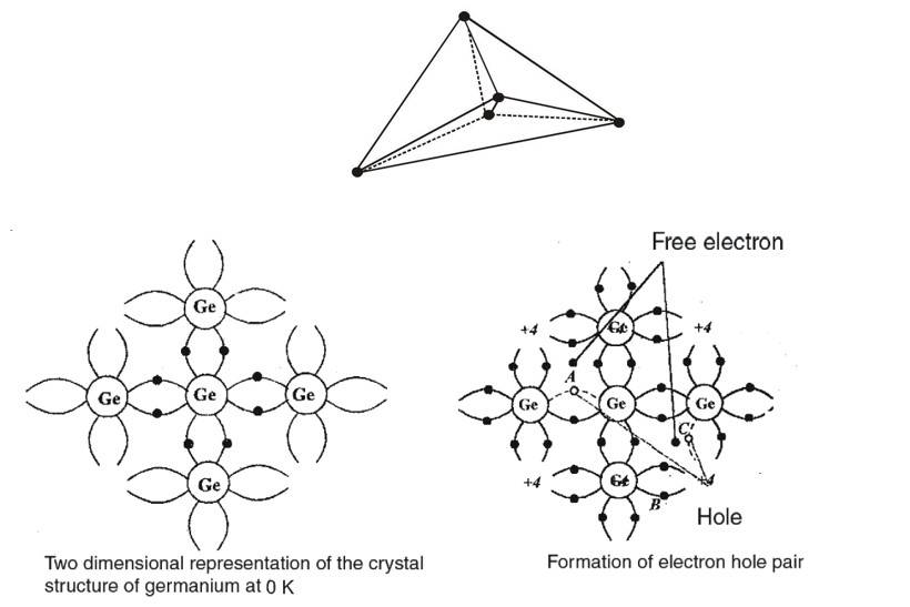
At , all the valence electrons are involved in the bonding and so the crystal is a perfect insulator as there are no free electrons available for conduction. At higher temperatures, however, some of the valence electrons have sufficient energy to break away from the bond and move in the crystal in random manner. Under an applied electric field these electrons drift and conduct electricity.
When an electron escapes from a band it leaves behind a vacancy in the lattice. This vacancy is termed as a "hole". The absence of electron amounts to the presence of a positive charge of same magnitude. As explained later, holes also take part in conduction in semiconductors. When a covalent bond is broken, all electron- hole pair is contributed.
At room temperature (300K) many electron - hole pairs are present in the crystal. The process of electron - hole generation is explained in figure. Let due to thermal energy an electron is set free from the covalent bond at site A whereby a hole is created at this site. An electron from the covalent bond of a neighbouring atom site may jump to vacant site then bond is completed at but a hole is created at . In this process a very small energy is involved compared to what is required for an electron - hole pair generation. It is because the electron is jumping from one bond to the other and all electrons in bonding are on an average of same energy. As shown in the figure when an electron jumps from to a hole is created at and so on. In effect then such a vacancy or hole can be considered as mobile. Thus in a semiconductor both electrons and holes act as charge carriers and contribute in electric conduction.
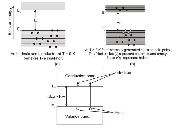
The number of electrons and holes generated by thermal means is equal for an intrinsic semiconductor. If and represents the electron and hole concentrations respectively then
Here is intrinsic charge carriers concentration.
Note :
(1) A pure semiconductor is called intrinsic semiconductor. It has thermally generated current carriers.
(2) They have four electrons in the outermost orbit of atom and atoms are held together by covalent bond.
(3) Free electrons and holes both are charge carriers and
(in C.B.)
(in V.B.)
(4) The drift velocity of electrons
is greater than that of holes
.
(5) For them fermi energy level lies at the centre of the C.B. and V.B.
(6) In pure semiconductor, impurity must be less than 1 in
parts of semiconductor.
(7) In intrinsic semiconductor
; where Electron density in conduction band,
Hole density in V.B.
, Density of intrinsic carriers.
(8) The fraction of electron of valance band present in conduction band is given by
; where
Fermi energy,
Boltzmann's constant and
Absolute temperature.
(9) Because of less number of charge carriers at room temperature, intrinsic semiconductors have low conductivity so they have no particle use.
(10) Number of electrons reaching from valence band to conduction band
where
is positive constant.
(11) Net charge of a pure semiconductor is zero.
Working Principle of Intrinsic Semiconductor
Let us understand how an intrinsic semiconductor works by taking the example of silicon.
- A silicon atom has 4 electrons in its outermost shell but needs 8 electrons to complete its octet.
- To achieve this, a silicon atom starts sharing electrons with neighbouring Silicon atoms to form covalent bonds. This completes its octet.
- At 0 kelvin (which is also known as absolute zero), an intrinsic semiconductor behaves like a perfect insulator because there is insufficient thermal energy for electrons to break free from their covalent bonds.
- As the temperature increases, the electron within the covalent bond breaks free and it is known as a ‘free electron’. A hole is created at the place where the free electron leaves its original place.
- As the number of free electrons increases, the number of holes also increases. This increases the number of charge carriers (electrons and holes), due to which the conductivity in the intrinsic semiconductors increases.
Difference Between Intrinsic and Extrinsic Semiconductors
Intrinsic and extrinsic semiconductors are distinguished based on the following parameters.
| Feature |
Intrinsic Semiconductor |
Extrinsic Semiconductor |
| Definition |
Pure semiconductor without impurities |
Doped semiconductor with added impurities |
| Example Materials |
Silicon (Si), Germanium (Ge) |
Doped Si or Ge with P, As, B, Al |
| Conductivity |
Low (due to few charge carriers) |
High (more free carriers due to doping) |
| Charge Carriers |
Equal number of electrons and holes |
Unequal — either electrons (n-type) or holes (p-type) |
| Source of Carriers |
Thermally generated electron-hole pairs |
Carriers provided by dopant atoms |
| Types |
Only one form |
Two: n-type and p-type |
| Temperature Dependence |
Highly temperature-dependent |
Less affected due to already available carriers |
| Application |
Basic research, temperature sensors |
Diodes, transistors, solar cells, LEDs and ICs |
Intrinsic Semiconductor Equations
1. Intrinsic Carrier Concentration (ni)
The most fundamental equation describes how many charge carriers exist per unit volume in an intrinsic semiconductor at a given temperature and how this number will increase with heat or shrink with a large bandgap.:
Where:
- ni = intrinsic carrier concentration (electrons/cm³)
- Nc = effective density of states in the conduction band (how many quantum states are available for electrons to occupy)
- Nv = effective density of states in the valence band
- Eg = band gap energy (eV) (energy needed for electrons to jump from valence to conduction band)
- k = Boltzmann's constant (8.617 × 10⁻⁵ eV/K)
- T = absolute temperature (in Kelvin)
- e = Exponential function base (≈ 2.718...)
In conclusion:
- The higher the temperature T, the more electrons will get excited → ni increases
- The wider the bandgap Eg, the harder it is for electrons to jump → ni decreases
- ni is very sensitive to temperature due to the exponential term.
2. Mass Action Law
n × p = ni²
The law states that even when you add impurities to an intrinsic semiconductor, the product of n x p is always equal to the square of the intrinsic carrier concentration ni² at a given temperature.
For intrinsic semiconductors:
Where:
- n = electron concentration
- p = hole concentration
- ni = intrinsic carrier concentration
In an intrinsic semiconductor, n = p = ni.
Case 1: Added Extra Electrons
Let us suppose that you have added impurities in the silicon to increase the number of electrons (n-type). Due to this doping, the n goes up, but since the law of mass action must be followed, the holes decrease proportionally.
Case 2: Added Holes
In this case, you will add atoms that have 1 less electron than required. Say, you add Boron atoms to silicon. Boron has only 3 valence electrons. This creates holes due to the missing electron. To maintain n × p = ni², electrons (n) will go down while p will go up.
Examples of Intrinsic Semiconductor
Intrinsic Semiconductor Questions in JEE Main and NEET
Frequently Asked Questions on Intrinsic Semiconductor
Physics Semiconductor Devices Exam
Student Forum
Other Class 12th Physics Chapters
- Physics Alternating Current
- Physics Ray Optics and Optical Instruments
- Physics Electromagnetic Induction
- Physics Dual Nature of Radiation and Matter
- Physics Semiconductor Devices
- Physics Wave Optics
- Physics Current Electricity
- Physics Nuclei
- Physics Electrostatic Potential and Capacitance
- Physics Atoms
- Physics Moving Charges and Magnetism
- NCERT Class 12 Notes
- NCERT Class 12 Physics
- Physics Electric Charge and Field
- Physics Electromagnetic Waves
- Physics Magnetism and Matter