 / Preparation Physics Ncert Solutions Class 12th
Chapter 14, Semiconductor Electronics covers the essentials of semiconductors, which form the foundation for modern electronic devices like transistors, diodes, and integrated circuits. Chapter 14 Physics Class 12 provides step-by-step solutions for NCERT textbook questions, simplifying the complex concepts of the chapter, like rectification, p-n junctions, and amplification.
This page also provides the Semiconductor Class 12 PDF. Students must download it for the CBSE Board examination and competitive examination preparation. The solutions include clear explanations, key notes, and practical insights for students.
These are some of the important topics covered in Chapter 14 Semiconductor Electronics:
- Semiconductor materials and their properties
- p-n junction formation and behavior
- Diode applications as rectifiers
- Energy band theory in solids
- Intrinsic and extrinsic semiconductors
For accessing all chapters of Class 12 Physics at one place with the important topics, free PDFs and weightage information, do read here - NCERT Solutions for Class 12 Physics.
- Inside Chapter 14 Semiconductor Electronics – Class 12 Physics Summary
- NCERT Solutions for Class 12 Physics Chapter 14 Semiconductor Electronics PDF
- Semiconductor Electronics: Materials, Devices and Simple Circuits Questions and Answers
- NCERT Solutions for Class 12 Physics Semiconductor Electronics: Key Topics and Weightage
- Benefits of Using Class 12 Physics Semiconductor Electronics Solutions
- NCERT Class 12 Physics Semiconductor Electronics Solutions- FAQs
Inside Chapter 14 Semiconductor Electronics – Class 12 Physics Summary
See below a quick walkthrough of this chapter:
Semiconductors, unlike vacuum, control electron flow within solids, offer low power consumption, have compact size, and high reliability for modern electronics like transistors and diodes. Three types of solids- metals with high conductivity, insulators with low conductivity and semiconductors with median conductivity. The semiconductors silicon and germanium are mostly used in electronic devices. p-n Junction is created by joining two types of semiconductors - p-type and n-type. It controls the current flow based on applied voltage by creating a depletion region with a potential barrier. A p-n junction diode is used in half-wave and full-wave rectifiers. It allows current in one direction. It is used to convert alternating current to direct current, with filters smoothing the output. Electron energy levels in solids form bands. The semiconductors have a small energy gap between the filled valence band and the empty conduction band. It enables the electron movement at room temperature.
NCERT Solutions for Class 12 Physics Chapter 14 Semiconductor Electronics PDF
Download the Semiconductor NCERT PDF from the link given below. It provides step-by-step answers to all textbook questions on important topics, including semiconductors, diodes, p-n junctions, and transistors.
Related Links
| NCERT Solutions for Class 12 Physics | NCERT Solutions Class 11 and 12 for Maths, Physics, Chemistry |
| NCERT Class 12 Notes | NCERT Class 12 Physics Notes for CBSE |
Semiconductor Electronics: Materials, Devices and Simple Circuits Questions and Answers
| Q.14.1 In an n-type silicon, which of the following statement is true: (a) Electrons are majority carriers and trivalent atoms are the dopants. (b) Electrons are minority carriers and pentavalent atoms are the dopants. (c) Holes are minority carriers and pentavalent atoms are the dopants. (d) Holes are majority carriers and trivalent atoms are the dopants. |
| Ans.14.1 The correct statement is (c ). In an n-type silicon, the electrons are the majority carrier, while the holes are the minority carriers. An n-type semiconductor is obtained when pentavalent atoms, such as phosphorous, are doped in silicon atoms. |
| Q.14.2 Which of the statements given in Exercise 14.1 is true for p-type semiconductor. |
| Ans. 14.2 The correct statement is (d). In a p-type semiconductor, the holes are the majority carriers, while the electrons are the minority carriers. A p-type semiconductor is obtained when trivalent atoms, such as aluminium, are doped in silicon atoms. |
| Q.14.3 Carbon, silicon and germanium have four valence electrons each. These are characterized by valence and conduction bands separated by energy band gap respectively equal to , and . Which of the following statements is true? (a) < < (b) < > (c) > > (d) = = |
| Ans.14.3 The correct statement is (c). Of the three given elements, the energy band gap of carbon is the maximum and germanium is the least. The energy band gap of these elements is related to > > |
| Q.14.4 In an unbiased p-n junction, holes diffuse from the p-region to n-region because (a) Free electrons in the n-region attract them. (b) They move across the junction by the potential difference. (c) Hole concentration in p-region is more as compared to n-region. (d) All the above. |
| Ans.14.4 The correct statement is (c). The diffusion of charge carriers across a junction takes place from the regions of higher concentration to the region of lower concentration. In this case, the p-region has greater concentration of holes than the n-region. Hence, in an unbiased p-n junction, holes diffuse from the p-region to the n-region. |

Commonly asked questions
14.8 The number of silicon atoms per m3 is 5 × 1028. This is doped simultaneously with 5 × 10²² atoms per m3 of Arsenic and 5 × 10²⁰ per m3 atoms of Indium. Calculate the number of electrons and holes. Given that ni = 1.5 × 10¹⁶ m–3. Is the material n type or p type?
14.8 Number of silicone atoms, = 5 /
Number of arsenic atoms, = 5 /
Number of indium atoms, = 5 /
Number of thermally generated atoms, = 1.5 /
Hence number of electrons, = 5 1.5 = 4.99
Number of holes =
In thermal equilibrium, the concentration of electrons and holes in a semiconductor are related as:
=
Therefore, = = = 4.51
Since the number of electrons are more (4.99 than the number of holes (4.51 , the material is an n-type semiconductor.
14.6 In half-wave rectification, what is the output frequency if the input frequency is 50 Hz. What is the output frequency of a full-wave rectifier for the same input frequency.
14.6 Input frequency = 50 Hz
For a half-wave rectifier, the output frequency is equal to the input frequency.
Hence, the output frequency = 50 Hz
For a full-wave rectifier, the output frequency is twice the input frequency.
Hence the output frequency = 2
14.9 In an intrinsic semiconductor the energy gap Eg is 1.2eV. Its hole mobility is much smaller than electron mobility and independent of temperature. What is the ratio between conductivity at 600K and that at 300K? Assume that the temperature dependence of intrinsic carrier concentration is given by
where is a constant.
14.9 Energy gap of the given intrinsic semiconductor, = 1.2 eV
The temperature dependence of the intrinsic carrier-concentration is written as:
Where, = Boltzmann constant = 8.62
eV/K
T = Temperature
= constant
Initial temperature,
= 300 K
The intrinsic carrier-concentration at this temperature can be written as
……(1)
Final temperature, = 600 K
The intrinsic carrier-concentration at this temperature can be written as
……(2)
The ratio between conductivity at 600K and at 300 K is equal to the ratio between the respective intrinsic carrier concentration at these temperatures.
Therefore,
=
= exp
= exp
= exp = exp(11.6) = 109
Therefore, the ratio between two conductivities is 1.09
14.10 In a p-n junction diode, the current I can be expressed as
where I0 is called the reverse saturation current, V is the voltage across the diode and is positive for forward bias and negative for reverse bias, and I is the current through the diode,
is the Boltzmann constant (8.6×10⁻⁵ eV/K) and T is the absolute temperature. If for a given diode I0 = 5 × 10–12 A and T = 300 K, then
(a) What will be the forward current at a forward voltage of 0.6 V?
(b) What will be the increase in the current if the voltage across the diode is increased to 0.7 V?
(c) What is the dynamic resistance?
(d) What will be the current if reverse bias voltage changes from 1 V to 2 V?
14.10 In a p-n junction diode, the expression for current is given as:
Where, = Reverse saturation current = 5 A
T = Absolute temperature = 300 K
= Boltzmann constant = 8.6 eV/K = 8.6 J/K = 1.376
V = voltage across the diode
e = charge of an electron = 1.6 C
Forward voltage, V = 0.6V
Current, =
= 0.02315 A
For forward voltage, V = 0.7V, we can write
Current, =
= 1.117 A
Hence increase in the current, ΔI = I’-I = 1.117 – 0.02315 = 1.0934 A
Dynamic resistance = =
If the reverse bias voltage is changed from 1 V to 2 V, the current will remain same as will be equal in both cases. Therefore the dynamic resistance in the reverse bias will be
14.4 In an unbiased p-n junction, holes diffuse from the p-region to n-region because
(a) free electrons in the n-region attract them.
(b) they move across the junction by the potential difference.
(c) hole concentration in p-region is more as compared to n-region.
(d) All the above.
14.4 The correct statement is (c).
The diffusion of charge carriers across a junction takes place from the regions of higher concentration to the region of lower concentration. In this case, the p-region has greater concentration of holes than the n-region. Hence, in an unbiased p-n junction, holes diffuse from the p-region to the n-region.
14.7 A p-n photodiode is fabricated from a semiconductor with band gap of 2.8 eV. Can it detect a wavelength of 6000 nm?
14.7 Energy band gap of the given photodiode, = 2.8 eV
Wavelength, = 6000 nm = 6000 m
The energy of a signal is given by the relation,
=
Where
h = Planck’s constant = 6.626 Js
c = sped of light = 3 m/s
= = 3.313 J = eV = 0.207 eV
Therefore the energy of a signal of wavelength 6000 nm is 0.207 eV, which is less than 2.8 eV – the energy band gap of the photodiode. Hence, the photodiode cannot detect the signal.
14.15 Write the truth table for the circuits given in Fig. 14.40 consisting of NOR gates only. Identify the logic operations (OR, AND, NOT) performed by the two circuits.

14.15 A acts as two inputs of the NOR gate and Y is the output. As shown in the following figure. Hence the output of the circuit is =

The truth table for the same is given as:
A | Y = ( ) |
0 | 1 |
1 | 0 |
This is the truth table of a NOT gate. Hence, this circuit functions as a NOT gate.
A and B are the inputs and Y is the output of the given circuit. By using the result obtained in solution (a), we can infer that the outputs of the first two NOR gates are and , as shown in the following figure

Above is given the inputs for the last NOR gate.
Hence, the output for the circuit can be written as:
Y = = = A.B
The truth table for the same can be written as:
A | B | Y(=A!B) |
0 | 0 | 0 |
0 | 1 | 0 |
1 | 0 | 0 |
1 | 1 | 1 |
This is the truth table of an AND gate. Hence, this circuit functions as an AND gate.
14.14 Write the truth table for circuit given in Fig. 14.39 below consisting of NOR gates and identify the logic operation (OR, AND, NOT) which this circuit is performing.

(Hint: A = 0, B = 1 then A and B inputs of second NOR gate will be 0 and hence Y=1. Similarly work out the values of Y for other combinations of A and B. Compare with the truth table of OR, AND, NOT gates and find the correct one.)
14.14 A and B are the inputs of the given circuit. The output of the first NOR gate is + . It can be observed from the following figure that the inputs of the second NOR gate become the output of the first one.

Hence, the output of the combination is given as:
Y = = + = = = + =
The truth table for this operation is given as:
This is the truth table of an or gate. Hence, this circuit functions as an or gate.
A | B | Y ( = A + B) |
0 | 0 | 0 |
0 | 1 | 1 |
1 | 0 | 1 |
1 | 1 | 1 |
This is the truth table of an OR gate. Hence, this circuit functions as an OR gate.
14.5 When a forward bias is applied to a p-n junction, it
(a) raises the potential barrier.
(b) reduces the majority carrier current to zero.
(c) lowers the potential barrier.
(d) None of the above.
14.5 The correct statement is (c).
When a forward bias is applied to a p-n junction, it lowers the value of potential barrier. In the case of a forward bias, the potential barrier opposes the applied voltage. Hence, the potential barrier across the junction gets reduced.
14.1 In an n-type silicon, which of the following statement is true:
(a) Electrons are majority carriers and trivalent atoms are the dopants.
(b) Electrons are minority carriers and pentavalent atoms are the dopants.
(c) Holes are minority carriers and pentavalent atoms are the dopants.
(d) Holes are majority carriers and trivalent atoms are the dopants.
14.1 The correct statement is (c ).
In an n-type silicon, the electrons are the majority carrier, while the holes are the minority carriers. An n-type semiconductor is obtained when pentavalent atoms, such as phosphorous, are doped in silicon atoms.
14.11 You are given the two circuits as shown in Fig. 14.36. Show that circuit (a) acts as OR gate while the circuit (b) acts as AND gate.
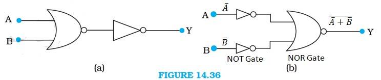
14.11 A and B are the inputs and Y is the output of the given circuit. The left half of the given figure acts as the NOR gate, while the right half acts as the NOT gate

Hence the output of the NOR gate is
This will be input for the NOT gate. Its output will be = A + B
So Y = A + B
Hence, this circuit functions as an OR gate.
A and B are the inputs and Y is the output of the given circuit. It can be observed from the following figure that the inputs of the right half NOR gate are the outputs of the two NOT gates.

Hence, the output of the given circuit can be written as:
Y = = = A + BHence this circuit functions as an AND gate.
14.12 Write the truth table for a NAND gate connected as given in Fig. 14.37.

Hence identify the exact logic operation carried out by this circuit.
14.12 A acts as the two inputs of the NAND gate and Y is the output, as shown in the following figure.

Hence, the output can be written as:
Y = = + = ……………(i)
The truth table for equation (i) can be drawn as:
A | Y = ( ) |
0 | 1 |
1 | 0 |
This circuit functions as a NOT gate. The symbol for this logic circuit is as shown below:

14.13 You are given two circuits as shown in Fig. 14.38, which consist of NAND gates. Identify the logic operation carried out by the two circuits.
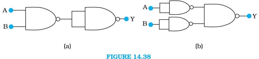
14.13 The output of the left NAND gate will be , as shown in the following figure:

Hence, the output of the combination of two NAND gates is given as:
Y = ( ).( ) = + = AB
Hence the circuit functions as an AND gate.
is the output of the upper left of the NAND gate and is the output of the lower half of the NAND gate, as shown in the following figure.

Hence, the output of the combination of the NAND gates will be given as:
Y = . = + = A + B
Hence, this circuit functions as an OR gate.
14.2 Which of the statements given in Exercise 14.1 is true for p-type semiconductor.
14.2 The correct statement is (d).
In a p-type semiconductor, the holes are the majority carriers, while the electrons are the minority carriers. A p-type semiconductor is obtained when trivalent atoms, such as aluminium, are doped in silicon atoms.
NCERT Solutions for Class 12 Physics Semiconductor Electronics: Key Topics and Weightage
You need to learn all the topics in this chapter, the Semiconductor Electronics topics like diode, transistor, and logic gates in class 12 Physics, are really important for competitive exams like NEET and JEE Main exams. The following topics are covered in thechapter 14:
| NCERT Section | Topic Covered |
|---|---|
| 14.1 | Introduction |
| 14.2 | Classification Of Metals, Conductors And Semiconductors |
| 14.3 | Intrinsic Semiconductor |
| 14.4 | Extrinsic Semiconductor |
| 14.5 | P-N Junction |
| 14.6 | Semiconductor Diode |
| 14.7 | Application of a Junction Diode as a Rectifier |
| 14.8 | Special Purpose p-n Junction Diodes |
| 14.9 | Junction Transistor |
| 14.10 | Digital Electronics and Logic Gates |
| 14.11 | Integrated Circuits |
Other Key Sub-Topics in This Chapter
- Energy Bands: Valence and Conduction Band
- Impurity and Extrinsic Conductor
- Schematic model
- N-type and P-type Semiconductor
- Stopping Potential
Benefits of Using Class 12 Physics Semiconductor Electronics Solutions
Shiksha offers detailed solutions for the NCERT Textbook exercise for Semiconductor Electronics.
- Subject Matter experts at Shiksha have carefully designed the solutions with accurate and step-by-step explanations, best suited for CBSE Board Exams.
- This chapter contains many important formulas and concepts. Our NCERT Solutions contain the best usage of these concepts and techniques to solve the problem in the required time.
- Students without internet access throughout the day can download the Semiconductor Electronics NCERT Solutions PDF to study offline.
- These Solutions provide a basic understanding of concepts, you can build advanced concepts over them to be used in competitive exams like JEE, NEET, and others
NCERT Class 12 Physics Semiconductor Electronics Solutions- FAQs
Students can check the frequently asked questions below;
Explore exams which ask questions on Physics Ncert Solutions Class 12th
Select your preferred stream
Physics Ncert Solutions Class 12th Exam
Student Forum
Other Similar chapters for you
- NCERT Physics 12th
- Electric Charges and Fields
- Electrostatic Potential and Capacitance
- Electricity
- Moving Charges and Magnetism
- Magnetism and Matter
- Electromagnetic Induction
- Alternating Current
- Electromagnetic Waves
- Ray Optics and Optical Instruments
- Wave Optics
- Dual Nature of Radiation and Matter
- Atoms
- Nuclei
- Semiconductor Electronics: Materials, Devices and
Popular Courses After 12th
Exams accepted
CA FoundationExams accepted
ICSI ExamExams accepted
BHU UET | GLAET | GD Goenka TestBachelor of Business Administration & Bachelor of Law
Exams accepted
CLAT | LSAT India | AIBEExams accepted
IPMAT | NMIMS - NPAT | SET
Exams accepted
BHU UET | KUK Entrance Exam | JMI Entrance ExamBachelor of Design in Animation (BDes)
Exams accepted
UCEED | NIFT Entrance Exam | NID Entrance ExamBA LLB (Bachelor of Arts + Bachelor of Laws)
Exams accepted
CLAT | AILET | LSAT IndiaBachelor of Journalism & Mass Communication (BJMC)
Exams accepted
LUACMAT | SRMHCAT | GD Goenka Test